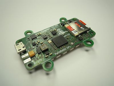
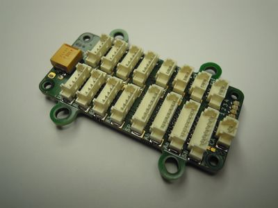
Tawaki/v1.00
Overview
Hardware Revision History
| Version # | Release Date | Release Notes |
|---|---|---|
| v1.00 | 07/2019 | Initial release of Tawaki |
Pictures
Detailed Features
MicroSD card (SDIO)
On-board Sensors
USB Modes
SWD: Serial Wire Debug
R/C Serial
Power
Communication Buses
LEDs
- 4x Leds classical Paparazzi state display
Pinout
Pins Name and Type are specified with respect to the Autopilot Board
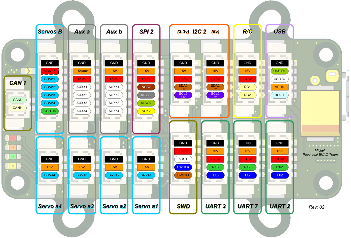
Simplified Pinout Diagram (Paparazzi use)
Simplified Pinout Tables(Paparazzi use)
UART2
| Pin # | Name | Type | MCU Port | Description |
|---|---|---|---|---|
| 1 | GND | PWR | - | common ground |
| 2 | +5V | PWR | - | 5V Rail from autopilot |
| 3 | +3.3V | PWR | - | 3.3V Rail from autopilot |
| 4 | RX2 | IN | PD6 | UART2 Serial Input (3.3V level) |
| 5 | TX2 | OUT | PD5 | UART2 Serial Output (3.3V level) |
UART3
| Pin # | Name | Type | MCU Port | Description |
|---|---|---|---|---|
| 1 | GND | PWR | - | common ground |
| 2 | +5V | PWR | - | 5V Rail from autopilot |
| 3 | +3.3V | PWR | - | 3.3V Rail from autopilot |
| 4 | RX2 | IN | PD9 | UART3 Serial Input (3.3V level) |
| 5 | TX2 | OUT | PD8 | UART3 Serial Output (3.3V level) |
UART7
| Pin # | Name | Type | MCU Port | Description |
|---|---|---|---|---|
| 1 | GND | PWR | - | common ground |
| 2 | +5V | PWR | - | 5V Rail from autopilot |
| 3 | +3.3V | PWR | - | 3.3V Rail from autopilot |
| 4 | RX2 | IN | PB3 | UART7 Serial Input (3.3V level) |
| 5 | TX2 | OUT | PA15 | UART7 Serial Output (3.3V level) |
I2C2 (3V3)
| Pin # | Name | Type | MCU Port | Description |
|---|---|---|---|---|
| 1 | GND | PWR | - | common ground |
| 2 | +5V | PWR | - | 5V Rail from autopilot |
| 3 | +3.3V | PWR | - | 3.3V Rail from autopilot |
| 4 | SDA2 3.3V | Open Drain I/O |
PB11 | I2C2 bus Serial DAta (3.3V level, 2.2kΩ pull-up) |
| 5 | SCL2 3.3V | Open Drain I/O |
PB10 | I2C12 bus Serial CLock (3.3V level, 2.2kΩ pull-up) |
I2C2 (5V)
| Pin # | Name | Type | MCU Port | Description |
|---|---|---|---|---|
| 1 | GND | PWR | - | common ground |
| 2 | +5V | PWR | - | 5V Rail from autopilot |
| 3 | +3.3V | PWR | - | 3.3V Rail from autopilot |
| 4 | SDA2 5V | Open Drain I/O |
PB11 | I2C2 bus Serial DAta (5V level, 2.2kΩ pull-up) |
| 5 | SCL2 5V | Open Drain I/O |
PB10 | I2C12 bus Serial CLock (5V level, 2.2kΩ pull-up) |
SPI2
| Pin # | Name | Type | MCU Port | Description |
|---|---|---|---|---|
| 1 | GND | PWR | - | common ground |
| 2 | +5V | PWR | - | 5V Rail from autopilot |
| 3 | +3.3V | PWR | - | 3.3V Rail from autopilot |
| 4 | NSS2 | OUT | PB12 | Slave Select. Selects the SPI slave |
| 5 | MOSI2 | I/O | PB15 | SPI2 Master Out Slave In. Data output from master / data input to slave |
| 6 | MISO2 | I/O | PB14 | SPI2 Master In Slave Out. Data input to master / data output from slave |
| 7 | SCK2 | I/O | PD3 | SPI2 Serial clock. Clock output from master or input to slave |
CAN
| Pin # | Name | Type | MCU Port | Description |
|---|---|---|---|---|
| 1 | CANL | I/O | - | CAN bidirectional - line |
| 2 | CANH | I/O | - | CAN bidirectional + line |
Note: Embedded 120Ω terminator resistor.
Servos a1 / a2 / a3 / a4
| Pin # | Name | Type | MCU Port | MCU Resource | Description |
|---|---|---|---|---|---|
| 1 | GND | PWR | - | - | common ground |
| 2 | +5V | PWR | - | - | 5V Rail from autopilot |
| 3 | SRVa1 SRVa2 SRVa3 SRVa4 |
OUT | PE9 PE11 PE13 PE14 |
Tim1.Ch1 Tim1.Ch2 Tim1.Ch3 Tim1.Ch4 |
Servo signal (PWM) |
Servos b
| Pin # | Name | Type | MCU Port | MCU Resource | Description |
|---|---|---|---|---|---|
| 1 | GND | PWR | - | - | common ground |
| 2 | VBAT | PWRIN/OUT | - | - | |
| 3 | SRVb1 | OUT | PB6 | Tim4.Ch1 | Servo signal (PWM) |
| 4 | SRVb2 | OUT | PB7 | Tim4.Ch2 | Servo signal (PWM) |
| 5 | SRVb2 | OUT | PB8 | Tim4.Ch3 | Servo signal (PWM) |
| 6 | SRVb2 | OUT | PB9 | Tim4.Ch4 | Servo signal (PWM) |
| 7 | DSHTin | IN | PB5 | UART5.Rx |
SWD
| Pin # | Name | Type | MCU Port | Description |
|---|---|---|---|---|
| 1 | GND | PWR | - | common ground |
| 2 | +3.3V | PWR | - | 3.3V Rail from autopilot |
| 3 | nRST | IN | - | MCU Reset (active low) |
| 4 | SWCLK | IN | PA14 | Serial Wire Clock |
| 5 | SWDIO | I/O | PA13 | Serial Wire Data Input/Output |
Schematic
Board production
Gerber & Drill for PCB
Bill Of Material
Components Layout
Pick-and-Place
Mechanical Dimensions
Programming
Debugging
Debugging with STM Discovery ST-LINK/V2 embedded debug tool
Debugging with CricketProbe
Source code
Available in latest git master branch.
Where to Buy
Check availability on Get Hardware page


