Difference between revisions of "Tawaki/v1.00"
(Fix Tx/Rx role for RC2 pin.) |
|||
| (30 intermediate revisions by one other user not shown) | |||
| Line 55: | Line 55: | ||
*Mechanical | *Mechanical | ||
** 53 x 25mm (2.1" x 0.98"), including 4x Φ2mm mounting holes (shares the same external dimensions and mounting points as Apogee) | ** 53 x 25mm (2.1" x 0.98"), including 4x Φ2mm mounting holes (shares the same external dimensions and mounting points as Apogee) | ||
** 4x Φ3mm extra mounting holes, 30 to 31mm spacing (30.5mm standard from Racers ESC, GPS modules, etc. ) | ** 4x Φ3mm extra mounting slotted holes, 30 to 31mm spacing (30.5mm standard from Racers ESC, GPS modules, etc. ) | ||
** 11g (0.4 oz) (including Micro-SD card) | ** 11g (0.4 oz) (including Micro-SD card) | ||
| Line 70: | Line 70: | ||
'''Servos a1 / a2 / a3 / a4''' | '''Servos a1 / a2 / a3 / a4''' | ||
{|border="1" cellspacing="0" style="text-align:center" cellpadding="2%" width="50%" | {|border="1" cellspacing="0" style="text-align:center" cellpadding="2%" width="50%" | ||
!width="3%"|''Pin #''!!width=" | !width="3%"|''Pin #''!!width="8%"|''Name''!!width="10%"|''Type''!!width="10%"|''MCU Port''!!width="15%"|''MCU Resource''!!''Description'' | ||
|- | |- | ||
|1||style="background:black; color:white"|GND||PWR||-||-||common ground | |1||style="background:black; color:white"|GND||PWR||-||-||common ground | ||
| Line 82: | Line 82: | ||
'''Servos b''' | '''Servos b''' | ||
{|border="1" cellspacing="0" style="text-align:center" cellpadding="2%" width="50%" | {|border="1" cellspacing="0" style="text-align:center" cellpadding="2%" width="50%" | ||
!width="3%"|''Pin #''!!width=" | !width="3%"|''Pin #''!!width="8%"|''Name''!!width="10%"|''Type''!!width="10%"|''MCU Port''!!width="15%"|''MCU Resource''!!''Description'' | ||
|- | |- | ||
|1||style="background:black; color:white"|GND||PWR||-||-||common ground | |1||style="background:black; color:white"|GND||PWR||-||-||common ground | ||
| Line 102: | Line 102: | ||
'''R/C''' | '''R/C''' | ||
{|border="1" cellspacing="0" style="text-align:center" cellpadding="2%" width="50%" | {|border="1" cellspacing="0" style="text-align:center" cellpadding="2%" width="50%" | ||
!width="3%"|''Pin #''!!width=" | !width="3%"|''Pin #''!!width="8%"|''Name''!!width="10%"|''Type''!!width="10%"|''MCU Port''!!width="15%"|''MCU Resource''!!''Description'' | ||
|- | |- | ||
|1||style="background:black; color:white"|GND||PWR||-||-||common ground | |1||style="background:black; color:white"|GND||PWR||-||-||common ground | ||
| Line 112: | Line 112: | ||
|4||style="background:LightYellow; color:black"|RC1||IN||PE0||UART8.Rx||(5V Tolerant) Serial (SBUS, Spektrum, etc.) | |4||style="background:LightYellow; color:black"|RC1||IN||PE0||UART8.Rx||(5V Tolerant) Serial (SBUS, Spektrum, etc.) | ||
|- | |- | ||
|5||style="background:LightYellow; color:black"|RC2||IN||PC6||UART6. | |5||style="background:LightYellow; color:black"|RC2||IN||PC6||UART6.Tx (use software swap to use it as Rx)<br>Tim3.Ch1<br>Tim8.Ch1||(5V Tolerant) Serial (SBUS, Spektrum, etc.) or PPM Stream RC receiver signal | ||
|} | |} | ||
<br> | <br> | ||
| Line 118: | Line 118: | ||
'''UART2''' | '''UART2''' | ||
{|border="1" cellspacing="0" style="text-align:center" cellpadding="2%" width="50%" | {|border="1" cellspacing="0" style="text-align:center" cellpadding="2%" width="50%" | ||
!width="3%"|''Pin #''!!width=" | !width="3%"|''Pin #''!!width="8%"|''Name''!!width="10%"|''Type''!!width="10%"|''MCU Port''!!''Description'' | ||
|- | |- | ||
|1||style="background:black; color:white"|GND||PWR||-||common ground | |1||style="background:black; color:white"|GND||PWR||-||common ground | ||
| Line 134: | Line 134: | ||
'''UART3''' | '''UART3''' | ||
{|border="1" cellspacing="0" style="text-align:center" cellpadding="2%" width="50%" | {|border="1" cellspacing="0" style="text-align:center" cellpadding="2%" width="50%" | ||
!width="3%"|''Pin #''!!width=" | !width="3%"|''Pin #''!!width="8%"|''Name''!!width="10%"|''Type''!!width="10%"|''MCU Port''!!''Description'' | ||
|- | |- | ||
|1||style="background:black; color:white"|GND||PWR||-||common ground | |1||style="background:black; color:white"|GND||PWR||-||common ground | ||
| Line 150: | Line 150: | ||
'''UART7''' | '''UART7''' | ||
{|border="1" cellspacing="0" style="text-align:center" cellpadding="2%" width="50%" | {|border="1" cellspacing="0" style="text-align:center" cellpadding="2%" width="50%" | ||
!width="3%"|''Pin #''!!width=" | !width="3%"|''Pin #''!!width="8%"|''Name''!!width="10%"|''Type''!!width="10%"|''MCU Port''!!''Description'' | ||
|- | |- | ||
|1||style="background:black; color:white"|GND||PWR||-||common ground | |1||style="background:black; color:white"|GND||PWR||-||common ground | ||
| Line 166: | Line 166: | ||
'''I2C2 (3V3)''' | '''I2C2 (3V3)''' | ||
{|border="1" cellspacing="0" style="text-align:center" cellpadding="2%" width="50%" | {|border="1" cellspacing="0" style="text-align:center" cellpadding="2%" width="50%" | ||
!width="3%"|''Pin #''!!width=" | !width="3%"|''Pin #''!!width="8%"|''Name''!!width="10%"|''Type''!!width="10%"|''MCU Port''!!''Description'' | ||
|- | |- | ||
|1||style="background:black; color:white"|GND||PWR||-||common ground | |1||style="background:black; color:white"|GND||PWR||-||common ground | ||
| Line 182: | Line 182: | ||
'''I2C2 (5V)''' | '''I2C2 (5V)''' | ||
{|border="1" cellspacing="0" style="text-align:center" cellpadding="2%" width="50%" | {|border="1" cellspacing="0" style="text-align:center" cellpadding="2%" width="50%" | ||
!width="3%"|''Pin #''!!width=" | !width="3%"|''Pin #''!!width="8%"|''Name''!!width="10%"|''Type''!!width="10%"|''MCU Port''!!''Description'' | ||
|- | |- | ||
|1||style="background:black; color:white"|GND||PWR||-||common ground | |1||style="background:black; color:white"|GND||PWR||-||common ground | ||
| Line 198: | Line 198: | ||
'''SPI2''' | '''SPI2''' | ||
{|border="1" cellspacing="0" style="text-align:center" cellpadding="2%" width="50%" | {|border="1" cellspacing="0" style="text-align:center" cellpadding="2%" width="50%" | ||
!width="3%"|''Pin #''!!width=" | !width="3%"|''Pin #''!!width="8%"|''Name''!!width="10%"|''Type''!!width="10%"|''MCU Port''!!''Description'' | ||
|- | |- | ||
|1||style="background:black; color:white"|GND||PWR||-||common ground | |1||style="background:black; color:white"|GND||PWR||-||common ground | ||
| Line 218: | Line 218: | ||
'''CAN''' | '''CAN''' | ||
{|border="1" cellspacing="0" style="text-align:center" cellpadding="2%" width="50%" | {|border="1" cellspacing="0" style="text-align:center" cellpadding="2%" width="50%" | ||
!width="3%"|''Pin #''!!width=" | !width="3%"|''Pin #''!!width="8%"|''Name''!!width="10%"|''Type''!!width="10%"|''MCU Port''!!''Description'' | ||
|- | |- | ||
|1||style="background:Green; color:white"|CANL||I/O||-||CAN bidirectional - line | |1||style="background:Green; color:white"|CANL||I/O||-||CAN bidirectional - line | ||
| Line 229: | Line 229: | ||
'''AUX a''' | '''AUX a''' | ||
{|border="1" cellspacing="0" style="text-align:center" cellpadding="2%" width="50%" | {|border="1" cellspacing="0" style="text-align:center" cellpadding="2%" width="50%" | ||
!width="3%"|''Pin #''!!width=" | !width="3%"|''Pin #''!!width="8%"|''Name''!!width="10%"|''Type''!!width="10%"|''MCU Port''!!width="15%"|''MCU Resource''!!''Description'' | ||
|- | |- | ||
|1||style="background:black; color:white"|GND||PWR||-||-||common ground | |1||style="background:black; color:white"|GND||PWR||-||-||common ground | ||
| Line 249: | Line 249: | ||
'''AUX b''' | '''AUX b''' | ||
{|border="1" cellspacing="0" style="text-align:center" cellpadding="2%" width="50%" | {|border="1" cellspacing="0" style="text-align:center" cellpadding="2%" width="50%" | ||
!width="3%"|''Pin #''!!width=" | !width="3%"|''Pin #''!!width="8%"|''Name''!!width="10%"|''Type''!!width="10%"|''MCU Port''!!width="15%"|''MCU Resource''!!''Description'' | ||
|- | |- | ||
|1||style="background:black; color:white"|GND||PWR||-||-||common ground | |1||style="background:black; color:white"|GND||PWR||-||-||common ground | ||
| Line 269: | Line 269: | ||
'''USB''' | '''USB''' | ||
{|border="1" cellspacing="0" style="text-align:center" cellpadding="2%" width="50%" | {|border="1" cellspacing="0" style="text-align:center" cellpadding="2%" width="50%" | ||
!width="3%"|''Pin #''!!width=" | !width="3%"|''Pin #''!!width="8%"|''Name''!!width="10%"|''Type''!!width="10%"|''MCU Port''!!''Description'' | ||
|- | |- | ||
|1||style="background:black; color:white"|GND||PWR||-||common ground | |1||style="background:black; color:white"|GND||PWR||-||common ground | ||
| Line 287: | Line 287: | ||
'''SWD''' | '''SWD''' | ||
{|border="1" cellspacing="0" style="text-align:center" cellpadding="2%" width="50%" | {|border="1" cellspacing="0" style="text-align:center" cellpadding="2%" width="50%" | ||
!width="3%"|''Pin #''!!width=" | !width="3%"|''Pin #''!!width="8%"|''Name''!!width="10%"|''Type''!!width="10%"|''MCU Port''!!''Description'' | ||
|- | |- | ||
|1||style="background:black; color:white"|GND||PWR||-||common ground | |1||style="background:black; color:white"|GND||PWR||-||common ground | ||
| Line 306: | Line 306: | ||
=== Power Supply === | === Power Supply === | ||
There are several ways to power the Tawaki board. '''CAUTION!''' use only one of these sources at a time: | |||
*with a battery or any power source that delivers between 6 and 17V | |||
*by connecting it to a USB port | |||
*with a power source that delivers a regulated, stable 5V | |||
Each of these methods is detailed below. | |||
==== | ==== Powering using battery/external source soldered onto battery pads ==== | ||
[[Image:Tawaki_v100_battery_pads_powering.png|600px|Tawaki v1.00 External source onto GND & VBAT pads]]<br><br> | |||
This is the basic setup: the Tawaki then generates all the internal power sources needed by its components. Additionally, the board provides +5V and +3.3V power sources through dedicated ports for external payload.<br> | |||
Limitations: | |||
*input power source range: 6-17V (2-4 Lipo cells) | |||
*maximum current usable by both Tawaki and payload on the +5V: I(5V)<4A | |||
*maximum current usable for payload on the +3.3V: I(3.3V)<3A | |||
*maximum total current usable: 4A | |||
[[Image:Tawaki_v100_servo_b_vbat_source.png|400px|Tawaki v1.00 Servos b header Vbat source for payload]]<br><br> | |||
With this setup, the external power source is available on the “VBAT” pin of the “Servos B” header - but only if solder bridge JP1 is jumped (turned ON) with a small blob of solder.<br> | |||
Limitation: | |||
*maximum current used on the “VBAT” pin must be less than 1A (because of the header’s specifications) | |||
==== | ==== Powering using battery/external source connected on "Servos B" header ==== | ||
==== | [[Image:Tawaki_v100_servo_b_header_powering.png|500px|Tawaki v1.00 External source on Servo b header]]<br><br> | ||
With this setup, the “GND”(-) and “VBAT”(+) pins of the “Servos B” header are used as the main entry ports for the external power source - but only if solder bridge JP1 is jumped (turned ON) with a small blob of solder. This can be interesting when the ESC already delivers the external power source voltage through its command and control signals (as is frequently the case on multi-rotors).<br> | |||
Limitations: <br> | |||
*input power source range: 6-17V (2-4 Lipo cells) | |||
*maximum total current usable: 1A (because of the header’s specifications) | |||
==== Powering using USB Micro-B only ==== | |||
[[Image:Tawaki_v100_Micro-B_USB_powering.png|1000px|Tawaki v1.00 USB Micro-B powering]]<br><br> | |||
It is possible to power the Tawaki with only a host computer, through the USB Micro-B port. This setup allows to power the board and all its components, while at the same time flashing it.<br> | |||
In this case, the "VBUS" pin of the "USB" header must be connected to the "+5V" pin of any header that is equipped with one - with the exception of the "5Vaux" pin of the "AUX a" header.<br> | |||
Limitation:<br> | |||
*the host computer must be capable of providing the current needed for: powering the board, and any potential external payload. With a maximum limit of 1A (because of the header’s specifications)<br> | |||
''Note: with this setup, the voltage of the external power source (VBAT) obviously cannot be measured by the micro-controller (MCU).'' | |||
==== Powering using external 5V source ==== | |||
[[Image:Tawaki_v100_external_5V_powering.png|800px|Tawaki v1.00 External 5V Source]]<br><br> | |||
In some cases the external power source is out of range and cannot be used, but an external 5V power source is available (for example provided by the ESC). In this case, the external 5V power source must be connected to the "+5V" and "GND" pins of any header that are equipped with them - with the exception of the "5Vaux" pin of the "AUX a" header.<br> | |||
Limitations:<br> | |||
*voltage range: 4-6V | |||
*the external 5V power source must be capable of providing the current needed for: powering the board, and any potential external payload. With a maximum limit of 1A (because of the headers' specifications) | |||
* the "VBUS" pin of the "USB" header must not be connected to the "+5V" pin of any header | |||
''Note: with this setup, the voltage of the external power source (VBAT) obviously cannot be measured by the micro-controller (MCU).'' | |||
=== USB Modes === | === USB Modes === | ||
==== Flash (DFU) mode ==== | |||
In this configuration, ''BOOT'' pin is connected to ''VBUS'' pin (#4 & #5 "USB" header).<br> | |||
If USB cable is plugged and autopilot is not powered or USB cable plugged before autopilot is powered, board enter DFU mode and is ready to be flashed.<br> | |||
[[Image:Tawaki_v100_USB_mode_DFU.png|600px|Tawaki v1.00 USB DFU/Flash mode]]<br> | |||
==== USB Storage mode ==== | |||
In this configuration, ''BOOT'' pin is connected to ''VBUS'' pin (#4 & #5 "USB" header).<br> | |||
If USB cable is plugged after autopilot is powered, autopilot task is stopped and board enters in USB storage mode to make SDcard content easily available by host as for an USB Pendrive. When unmounted and unplugged, autopilot task restart. | |||
[[Image:Tawaki_v100_USB_mode_storage.png|600px|Tawaki v1.00 USB Storage mode]]<br> | |||
==== Full Speed USB mode ==== | |||
=== General Pinout === | === General Pinout === | ||
| Line 325: | Line 379: | ||
=== Schematic === | === Schematic === | ||
=== Mechanical Dimensions === | === Mechanical === | ||
==== Mechanical Dimensions ==== | |||
[[Image:Tawaki_v100_top_mechanical_dimensions.png|800px|Tawaki v1.00 top mechanical dimensions]] | |||
==== CAD Files / 3D Model ==== | |||
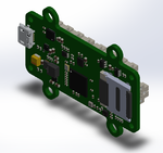
[[Image:Tawaki_v100_step_file_logo.PNG|150px|link=Tawaki_v100_CAD.zip]][[Media:Tawaki_v100_CAD.zip|'' Download Tawaki v1.00 CAD File (zipped STEP file)'']]<br> | |||
== Example of Airborne Equipment Electrical Connections == | |||
== Board production == | == Board production == | ||
| Line 334: | Line 398: | ||
=== Components Layout === | === Components Layout === | ||
[[Image:Tawaki_v100_bottom_components_layout.png|200px|link=https://wiki.paparazziuav.org/w/images/3/31/Tawaki_v100_bottom_components_layout.png]][[Media:Tawaki_v100_bottom_components_layout.pdf|Bottom components layout (pdf)]]<br> | |||
[[Image:Tawaki_v100_top_components_layout.png|200px|link=https://wiki.paparazziuav.org/w/images/c/ca/Tawaki_v100_bottom_components_layout.png]][[Media:Tawaki_v100_top_components_layout.pdf|Top components layout (pdf)]] | |||
=== Pick-and-Place === | === Pick-and-Place === | ||
Latest revision as of 08:28, 19 January 2021
Hardware Revision History
| Version # | Release Date | Release Notes |
|---|---|---|
| v1.00 | 07/2019 | Initial release of Tawaki |
Overview
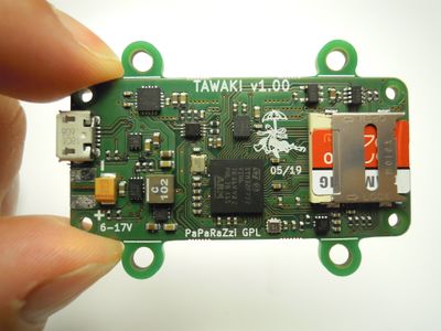
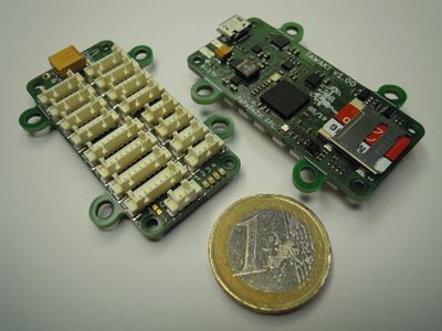
Pictures
Key Features
- STMicro STM32F777VI Micro Controller Unit
- ARM Cortex-M7, 216 MHz CPU, FPU & DSP instructions, 2 Mbytes Flash, 512 Kbytes SRAM, General-purpose DMA, HW Crypto,etc.
- On-board Sensors
- 8x Servos or ESC outputs (PWM/OneShot/DShot) + D-Shot Telemetry serial input
- 2x RC Receiver Inputs (S.BUS, PPM & Spektrum Satellite compatible, including receiver binding)
- Communication Buses
- 3x UARTs (including one with hardware flow control signals)
- 1x I2C bus (3.3V and 5V logic level)
- 1x SPI bus (with Slave Select, Master or Slave)
- 1x CAN bus
- 1x USB (Micro-B & remote) : DFU mode (download) or USB storage (direct access to MicroSD card) or FullSpeed Mode
- 8x Auxiliary Inputs/Outputs spread over 2 connectors (8x ADC, 8x Timers different from servos, x1 UART, etc.)
- MicroSD card (+ dedicated power supply for emergency files closing system)
- Debug Connector (Serial Wire Debug)
- Power
- source 2 to 4 Lipo cells (6 to 17v)
- 5V/4A (max total for Tawaki + Servos + Payload)
- 3.3V/3A Low Noise (max total for payload)
- Controlled PowerSwitch 5V/2A supply on AUX A connector
- x4 Status Leds
- Connectors fully compatible with Apogee autopilot
- Mechanical
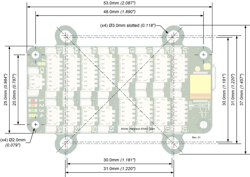
- 53 x 25mm (2.1" x 0.98"), including 4x Φ2mm mounting holes (shares the same external dimensions and mounting points as Apogee)
- 4x Φ3mm extra mounting slotted holes, 30 to 31mm spacing (30.5mm standard from Racers ESC, GPS modules, etc. )
- 11g (0.4 oz) (including Micro-SD card)
Pinout
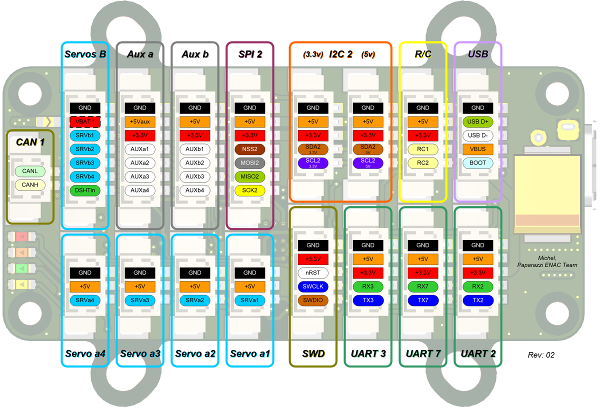
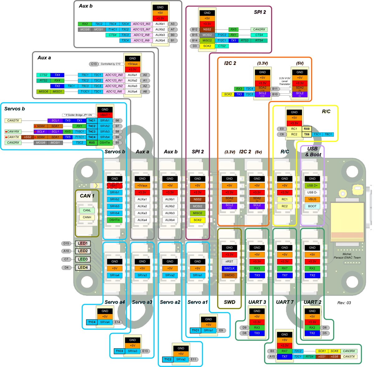
Simplified Pinout Diagram (Paparazzi use)
Pins Name and Type are specified with respect to the Autopilot Board
Simplified Pinout Tables (Paparazzi use)
Servos a1 / a2 / a3 / a4
| Pin # | Name | Type | MCU Port | MCU Resource | Description |
|---|---|---|---|---|---|
| 1 | GND | PWR | - | - | common ground |
| 2 | +5V | PWR | - | - | 5V Rail from autopilot |
| 3 | SRVa1 SRVa2 SRVa3 SRVa4 |
OUT | PE9 PE11 PE13 PE14 |
Tim1.Ch1 Tim1.Ch2 Tim1.Ch3 Tim1.Ch4 |
Servo signal (PWM) |
Servos b
| Pin # | Name | Type | MCU Port | MCU Resource | Description |
|---|---|---|---|---|---|
| 1 | GND | PWR | - | - | common ground |
| 2 | VBAT | PWRIN/OUT | - | - | Battery Rail (if solder bridge JP1 ON) |
| 3 | SRVb1 | OUT | PB6 | Tim4.Ch1 | Servo signal (PWM) |
| 4 | SRVb2 | OUT | PB7 | Tim4.Ch2 | Servo signal (PWM) |
| 5 | SRVb3 | OUT | PB8 | Tim4.Ch3 | Servo signal (PWM) |
| 6 | SRVb4 | OUT | PB9 | Tim4.Ch4 | Servo signal (PWM) |
| 7 | DSHTin | IN | PB5 | UART5.Rx | DShot Telemetry serial input |
R/C
| Pin # | Name | Type | MCU Port | MCU Resource | Description |
|---|---|---|---|---|---|
| 1 | GND | PWR | - | - | common ground |
| 2 | +5V | PWR | - | - | 5V Rail from autopilot |
| 3 | +3.3V | PWR | - | - | 3.3V Rail from autopilot |
| 4 | RC1 | IN | PE0 | UART8.Rx | (5V Tolerant) Serial (SBUS, Spektrum, etc.) |
| 5 | RC2 | IN | PC6 | UART6.Tx (use software swap to use it as Rx) Tim3.Ch1 Tim8.Ch1 |
(5V Tolerant) Serial (SBUS, Spektrum, etc.) or PPM Stream RC receiver signal |
UART2
| Pin # | Name | Type | MCU Port | Description |
|---|---|---|---|---|
| 1 | GND | PWR | - | common ground |
| 2 | +5V | PWR | - | 5V Rail from autopilot |
| 3 | +3.3V | PWR | - | 3.3V Rail from autopilot |
| 4 | RX2 | IN | PD6 | UART2 Serial Input (3.3V level) |
| 5 | TX2 | OUT | PD5 | UART2 Serial Output (3.3V level) |
UART3
| Pin # | Name | Type | MCU Port | Description |
|---|---|---|---|---|
| 1 | GND | PWR | - | common ground |
| 2 | +5V | PWR | - | 5V Rail from autopilot |
| 3 | +3.3V | PWR | - | 3.3V Rail from autopilot |
| 4 | RX2 | IN | PD9 | UART3 Serial Input (3.3V level) |
| 5 | TX2 | OUT | PD8 | UART3 Serial Output (3.3V level) |
UART7
| Pin # | Name | Type | MCU Port | Description |
|---|---|---|---|---|
| 1 | GND | PWR | - | common ground |
| 2 | +5V | PWR | - | 5V Rail from autopilot |
| 3 | +3.3V | PWR | - | 3.3V Rail from autopilot |
| 4 | RX2 | IN | PB3 | UART7 Serial Input (3.3V level) |
| 5 | TX2 | OUT | PA15 | UART7 Serial Output (3.3V level) |
I2C2 (3V3)
| Pin # | Name | Type | MCU Port | Description |
|---|---|---|---|---|
| 1 | GND | PWR | - | common ground |
| 2 | +5V | PWR | - | 5V Rail from autopilot |
| 3 | +3.3V | PWR | - | 3.3V Rail from autopilot |
| 4 | SDA2 3.3V | Open Drain I/O | PB11 | I2C2 bus Serial DAta (3.3V level, 2.2kΩ pull-up) |
| 5 | SCL2 3.3V | Open Drain I/O | PB10 | I2C12 bus Serial CLock (3.3V level, 2.2kΩ pull-up) |
I2C2 (5V)
| Pin # | Name | Type | MCU Port | Description |
|---|---|---|---|---|
| 1 | GND | PWR | - | common ground |
| 2 | +5V | PWR | - | 5V Rail from autopilot |
| 3 | +3.3V | PWR | - | 3.3V Rail from autopilot |
| 4 | SDA2 5V | Open Drain I/O | PB11 | I2C2 bus Serial DAta (5V level, 2.2kΩ pull-up) |
| 5 | SCL2 5V | Open Drain I/O | PB10 | I2C12 bus Serial CLock (5V level, 2.2kΩ pull-up) |
SPI2
| Pin # | Name | Type | MCU Port | Description |
|---|---|---|---|---|
| 1 | GND | PWR | - | common ground |
| 2 | +5V | PWR | - | 5V Rail from autopilot |
| 3 | +3.3V | PWR | - | 3.3V Rail from autopilot |
| 4 | NSS2 | OUT | PB12 | Slave Select. Selects the SPI slave |
| 5 | MOSI2 | I/O | PB15 | SPI2 Master Out Slave In. Data output from master / data input to slave |
| 6 | MISO2 | I/O | PB14 | SPI2 Master In Slave Out. Data input to master / data output from slave |
| 7 | SCK2 | I/O | PD3 | SPI2 Serial clock. Clock output from master or input to slave |
CAN
| Pin # | Name | Type | MCU Port | Description |
|---|---|---|---|---|
| 1 | CANL | I/O | - | CAN bidirectional - line |
| 2 | CANH | I/O | - | CAN bidirectional + line |
Note: Embedded 120Ω terminator resistor.
AUX a
| Pin # | Name | Type | MCU Port | MCU Resource | Description |
|---|---|---|---|---|---|
| 1 | GND | PWR | - | - | common ground |
| 2 | +5V Aux | PWR | (Controlled by) PC13 | - | 5V from autopilot through Power Switch (PC13 = Low => OFF / PC13 = High => ON) |
| 3 | +3.3V | PWR | - | - | 3.3V Rail from autopilot |
| 4 | AUXa1 | I/O | PA0 | ADC1+2+3.In0 Tim2.Ch1 Tim5.Ch1 UART4.Tx UART2.CTS |
General Purpose I/O |
| 5 | AUXa2 | I/O | PA1 | ADC1+2+3.In1 Tim2.Ch2 Tim5.Ch2 UART4.Rx UART2.RTS |
General Purpose I/O |
| 6 | AUXa3 | I/O | PA2 | ADC1+2+3.In2 Tim2.Ch3 Tim5.Ch3 Tim9.Ch1 |
General Purpose I/O |
| 7 | AUXa4 | I/O | PA6 | ADC1+2.In6 Tim3.Ch1 Tim13.Ch1 |
General Purpose I/O |
AUX b
| Pin # | Name | Type | MCU Port | MCU Resource | Description |
|---|---|---|---|---|---|
| 1 | GND | PWR | - | - | common ground |
| 2 | +5V | PWR | - | - | 5V Rail from autopilot |
| 3 | +3.3V | PWR | - | - | 3.3V Rail from autopilot |
| 4 | AUXb1 | I/O | PA3 | ADC1+2+3.In3 Tim2.Ch4 Tim5.Ch4 Tim9.Ch2 |
General Purpose I/O |
| 5 | AUXb2 | I/O | PA7 | ADC1+2+3.In7 Tim3.Ch2 Tim14.Ch1 |
General Purpose I/O |
| 6 | AUXb3 | I/O | PB0 | ADC1+2.In8 Tim3.Ch3 |
General Purpose I/O |
| 7 | AUXb4 | I/O | PB1 | ADC1+2.In9 Tim3.Ch4 |
General Purpose I/O |
USB
| Pin # | Name | Type | MCU Port | Description |
|---|---|---|---|---|
| 1 | GND | PWR | - | common ground |
| 2 | USB+ | I/O | PA12 | USB bidirectional D+ line |
| 3 | USB- | I/O | PA11 | USB bidirectional D- line |
| 4 | VBUS | IN | PA9 | USB bus power (5V) |
| 5 | BOOT | IN | BOOT0 | DFU or USB Mode selection (BOOT0 MCU pin) |
Note: USB Micro-B and Molex Picoblade connectors are in parallel, only one should be connected at a time.
SWD
| Pin # | Name | Type | MCU Port | Description |
|---|---|---|---|---|
| 1 | GND | PWR | - | common ground |
| 2 | +3.3V | PWR | - | 3.3V Rail from autopilot |
| 3 | nRST | IN | NRST | MCU Reset (active low) |
| 4 | SWCLK | IN | PA14 | Serial Wire Clock |
| 5 | SWDIO | I/O | PA13 | Serial Wire Data Input/Output |
Detailed Features
Power Supply
There are several ways to power the Tawaki board. CAUTION! use only one of these sources at a time:
- with a battery or any power source that delivers between 6 and 17V
- by connecting it to a USB port
- with a power source that delivers a regulated, stable 5V
Each of these methods is detailed below.
Powering using battery/external source soldered onto battery pads
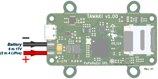
This is the basic setup: the Tawaki then generates all the internal power sources needed by its components. Additionally, the board provides +5V and +3.3V power sources through dedicated ports for external payload.
Limitations:
- input power source range: 6-17V (2-4 Lipo cells)
- maximum current usable by both Tawaki and payload on the +5V: I(5V)<4A
- maximum current usable for payload on the +3.3V: I(3.3V)<3A
- maximum total current usable: 4A
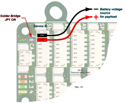
With this setup, the external power source is available on the “VBAT” pin of the “Servos B” header - but only if solder bridge JP1 is jumped (turned ON) with a small blob of solder.
Limitation:
- maximum current used on the “VBAT” pin must be less than 1A (because of the header’s specifications)
Powering using battery/external source connected on "Servos B" header
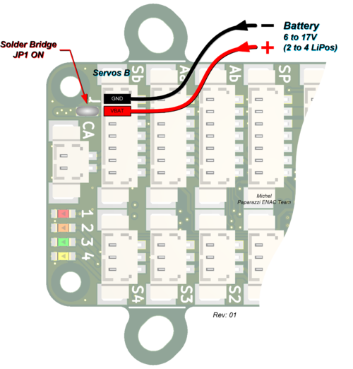
With this setup, the “GND”(-) and “VBAT”(+) pins of the “Servos B” header are used as the main entry ports for the external power source - but only if solder bridge JP1 is jumped (turned ON) with a small blob of solder. This can be interesting when the ESC already delivers the external power source voltage through its command and control signals (as is frequently the case on multi-rotors).
Limitations:
- input power source range: 6-17V (2-4 Lipo cells)
- maximum total current usable: 1A (because of the header’s specifications)
Powering using USB Micro-B only
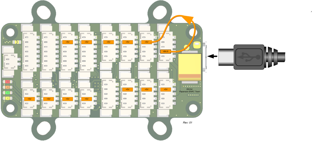
It is possible to power the Tawaki with only a host computer, through the USB Micro-B port. This setup allows to power the board and all its components, while at the same time flashing it.
In this case, the "VBUS" pin of the "USB" header must be connected to the "+5V" pin of any header that is equipped with one - with the exception of the "5Vaux" pin of the "AUX a" header.
Limitation:
- the host computer must be capable of providing the current needed for: powering the board, and any potential external payload. With a maximum limit of 1A (because of the header’s specifications)
Note: with this setup, the voltage of the external power source (VBAT) obviously cannot be measured by the micro-controller (MCU).
Powering using external 5V source
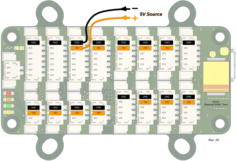
In some cases the external power source is out of range and cannot be used, but an external 5V power source is available (for example provided by the ESC). In this case, the external 5V power source must be connected to the "+5V" and "GND" pins of any header that are equipped with them - with the exception of the "5Vaux" pin of the "AUX a" header.
Limitations:
- voltage range: 4-6V
- the external 5V power source must be capable of providing the current needed for: powering the board, and any potential external payload. With a maximum limit of 1A (because of the headers' specifications)
- the "VBUS" pin of the "USB" header must not be connected to the "+5V" pin of any header
Note: with this setup, the voltage of the external power source (VBAT) obviously cannot be measured by the micro-controller (MCU).
USB Modes
Flash (DFU) mode
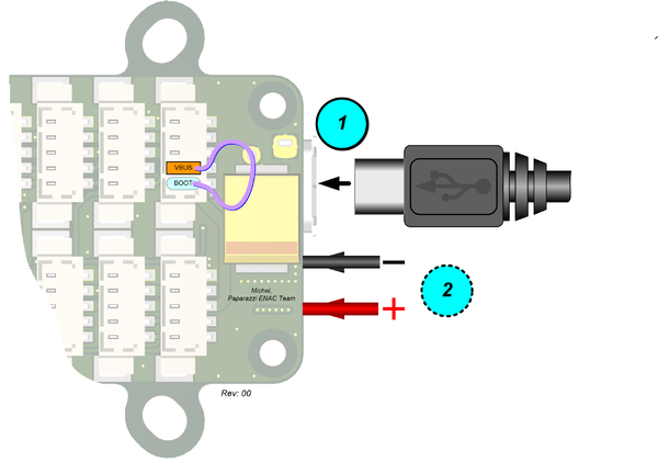
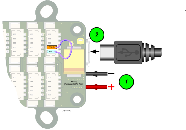
In this configuration, BOOT pin is connected to VBUS pin (#4 & #5 "USB" header).
If USB cable is plugged and autopilot is not powered or USB cable plugged before autopilot is powered, board enter DFU mode and is ready to be flashed.
USB Storage mode
In this configuration, BOOT pin is connected to VBUS pin (#4 & #5 "USB" header).
If USB cable is plugged after autopilot is powered, autopilot task is stopped and board enters in USB storage mode to make SDcard content easily available by host as for an USB Pendrive. When unmounted and unplugged, autopilot task restart.
Full Speed USB mode
General Pinout
Pins Name and Type are specified with respect to the Autopilot Board
Schematic
Mechanical
Mechanical Dimensions
CAD Files / 3D Model
Example of Airborne Equipment Electrical Connections
Board production
Gerber & Drill for PCB
Bill Of Material
Components Layout
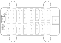 Bottom components layout (pdf)
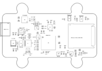 Top components layout (pdf)
Pick-and-Place
Programming
Debugging
Debugging with STM Discovery ST-LINK/V2 embedded debug tool
Debugging with BlackMagic probe
Debugging with CricketProbe
Source code
Available in latest git master branch.
Where to Buy
Check availability on Get Hardware page
