Difference between revisions of "STM32F4 Discovery"
(→THT) |
|||
| (42 intermediate revisions by 4 users not shown) | |||
| Line 1: | Line 1: | ||
'''This page is for the [http://www.st.com/web/catalog/tools/FM116/SC959/SS1532/PF252419 STM32F4 Discovery board with STM32F407VGT6], STM32F4 Disco is a familiar board with STM32F401VCT6, do not use this Files for the Disco board ! ''' | |||
{| align=right | |||
|- | |||
|<categorytree style="float:right; clear:right; margin-left:1ex; border: 1px solid gray; padding: 0.7ex;" mode=pages>Autopilots</categorytree> | |||
|} | |||
<div style="float: right; width: 65%"> | |||
[[Image:STM32F4Discovery_front.jpg|300px]] | |||
[[Image:STM32F4Discovery_back.jpg|300px]] | |||
</div> | |||
__TOC__ | |||
==Overview== | ==Overview== | ||
* STMicroelectronics STM32F4VGT6 Cortex M4 MCU, up to 168Mhz with floating point unit (FPU), 192 KB RAM, | |||
* on-board | * STMicroelectronics STM32F4VGT6 Cortex M4 MCU, up to 168Mhz with floating point unit (FPU), 192 KB RAM, 1024 KB Flash | ||
* | * on-board STLinkv2 with SWD header (capable of programming onboard or external MCU) | ||
* on-board power regulator for the MCU (3V or 5V Input) | |||
* 1 x user push button | * 1 x user push button | ||
* 4(5) x LED (orange, green, blue | * 4(5) x LED (orange, green, red, blue, green) | ||
* 6 x UART (UART1, UART2, UART3, UART4, UART5, UART6) | * 4(6) x UART (UART1, UART2, UART3, (UART4, UART5), UART6) | ||
* 3 x SPI (SPI1, SPI2, SPI3) | * 1(3) x SPI (SPI1, (SPI2, SPI3)) | ||
* 2(3) x I2C (I2C1, I2C2, (I2C3)) | * 2(3) x I2C (I2C1, I2C2, (I2C3)) | ||
* 6 x ADC inputs (one is used for BAT voltage) | |||
* 1 x PPM input | * 1 x PPM input | ||
* | * 1 x Spektrum input (with bind pin) | ||
* 97 x 66 mm PCB | * 97 x 66 mm PCB | ||
* 4 x status LED (USB | * 4 x status LED (USB red, USB green, power, USB OTG green, USB OTG red) | ||
* LIS302DL MEMS 3 axis accelerometer ( | * LIS302DL MEMS 3 axis accelerometer on SPI1 | ||
== Pinout == | |||
The Discovery has a male 100 pin (2x25pin on both sides, also accessible on both sides of the pcb) pinout. | |||
{|border="1" cellspacing="0" style="text-align:center" cellpadding="2%" width="60%" | |||
|+'''LED''' | |||
!width="7%"|''Pin #''!!width="10%"|''Name''!!width="10%"|''Type''!!''Description''!!width="5%"|''Color'' | |||
|- | |||
|PD13||LED_3||Out||above LIS302DL||style="background:orange; color:black"|Orange | |||
|- | |||
|PD12||LED_4||Out||left of LIS302DL||style="background:green; color:black"|Green | |||
|- | |||
|PD14||LED_5||Out||right of LIS302DL||style="background:red; color:black"|Red | |||
|- | |||
|PD15||LED_6||Out||below LIS302DL||style="background:blue; color:black"|Blue | |||
|- | |||
|PA9||LED_9||Out||same as USB power (VBUS, needs to be enabled in header file)||style="background:green; color:black"|Green | |||
|} | |||
{|border="1" cellspacing="0" style="text-align:center" cellpadding="2%" width="60%" | |||
|+'''UART1''' | |||
!width="7%"|''Pin #''!!width="10%"|''Name''!!width="10%"|''Type''!!''Description'' | |||
|- | |||
|PB6||UART1 TX||Out||UART1 Serial Output, 4k7 pullup for I2C | |||
|- | |||
|PB7||UART1 RX||In||UART1 Serial Input | |||
|} | |||
{|border="1" cellspacing="0" style="text-align:center" cellpadding="2%" width="60%" | |||
|+'''UART2''' | |||
!width="7%"|''Pin #''!!width="10%"|''Name''!!width="10%"|''Type''!!''Description'' | |||
|- | |||
|PD5||UART2 TX||Out||UART2 Serial Output (usb otg power management fault output open drain) | |||
|- | |||
|PD6||UART2 RX||In||UART2 Serial Input, also used for Spektrum input | |||
|} | |||
{|border="1" cellspacing="0" style="text-align:center" cellpadding="2%" width="60%" | |||
|+'''UART3''' | |||
!width="7%"|''Pin #''!!width="10%"|''Name''!!width="10%"|''Type''!!''Description'' | |||
|- | |||
|PD8||UART3 TX||Out||UART3 Serial Output | |||
|- | |||
|PD9||UART3 RX||In||UART3 Serial Input | |||
|} | |||
{|border="1" cellspacing="0" style="text-align:center" cellpadding="2%" width="60%" | |||
|+'''UART4 (Can NOT be used if SPI_3 is active!)''' | |||
!width="7%"|''Pin #''!!width="10%"|''Name''!!width="10%"|''Type''!!''Description'' | |||
|- | |||
|PC10||UART4 TX||Out||UART4 Serial Output | |||
|- | |||
|PC11||UART4 RX||In||UART4 Serial Input | |||
|} | |||
{|border="1" cellspacing="0" style="text-align:center" cellpadding="2%" width="60%" | |||
|+'''UART5 (Can NOT be used if SPI_3 is active!)''' | |||
!width="7%"|''Pin #''!!width="10%"|''Name''!!width="10%"|''Type''!!''Description'' | |||
|- | |||
|PC12||UART5 TX||Out||UART5 Serial Output | |||
|- | |||
|PD2||UART5 RX||In||UART5 Serial Input | |||
|} | |||
{|border="1" cellspacing="0" style="text-align:center" cellpadding="2%" width="60%" | |||
|+'''UART6''' | |||
!width="7%"|''Pin #''!!width="10%"|''Name''!!width="10%"|''Type''!!''Description'' | |||
|- | |||
|PC6||UART6 TX||Out||UART6 Serial Output | |||
|- | |||
|PC7||UART6 RX||In||UART6 Serial Input | |||
|} | |||
{|border="1" cellspacing="0" style="text-align:center" cellpadding="2%" width="60%" | |||
|+'''SPI1 (for onboard LIS302DL)''' | |||
!width="7%"|''Pin #''!!width="10%"|''Name''!!width="10%"|''Type''!!''Description'' | |||
|- | |||
|PA5||SPI1 SCK||I/O||SPI1 Serial clock | |||
|- | |||
|PA6||SPI1 MISO||I/O||SPI1 Master In Slave Out | |||
|- | |||
|PA7||SPI1 MOSI||I/O||SPI1 Master Out Slave In | |||
|- | |||
|PE3||SPI SS2||I/O||SPI1 Select Slave2 | |||
|} | |||
{|border="1" cellspacing="0" style="text-align:center" cellpadding="2%" width="60%" | |||
|+'''SPI1''' | |||
!width="7%"|''Pin #''!!width="10%"|''Name''!!width="10%"|''Type''!!''Description'' | |||
|- | |||
|PB3||SPI1 SCK||I/O||SPI1 Serial clock | |||
|- | |||
|PB4||SPI1 MISO||I/O||SPI1 Master In Slave Out | |||
|- | |||
|PB5||SPI1 MOSI||I/O||SPI1 Master Out Slave In | |||
|- | |||
|PE2||SPI SS0||I/O||SPI1 Select Slave0 | |||
|} | |||
{|border="1" cellspacing="0" style="text-align:center" cellpadding="2%" width="60%" | |||
|+'''SPI2 (Can NOT be used if PWM10 & PWM11 is active!)''' | |||
!width="7%"|''Pin #''!!width="10%"|''Name''!!width="10%"|''Type''!!''Description'' | |||
|- | |||
|PB13||SPI2 SCK||I/O||SPI2 Serial clock | |||
|- | |||
|PB14||SPI2 MISO||I/O||SPI2 Master In Slave Out | |||
|- | |||
|PB15||SPI2 MOSI||I/O||SPI2 Master Out Slave In | |||
|- | |||
|PE7||SPI SS1||I/O||SPI2 Select Slave1 | |||
|} | |||
{|border="1" cellspacing="0" style="text-align:center" cellpadding="2%" width="60%" | |||
|+'''SPI3 (Can NOT be used if UART4 & UART5 is active!)''' | |||
!width="7%"|''Pin #''!!width="10%"|''Name''!!width="10%"|''Type''!!''Description'' | |||
|- | |||
|PC10||SPI3 SCK||I/O||SPI3 Serial clock | |||
|- | |||
|PC11||SPI3 MISO||I/O||SPI3 Master In Slave Out | |||
|- | |||
|PC12||SPI3 MOSI||I/O||SPI3 Master Out Slave In | |||
|- | |||
|PE3||SPI SS2||I/O||SPI3 Select Slave2 (also used for LIS302DL (SPI1) Slave Select) | |||
|} | |||
{|border="1" cellspacing="0" style="text-align:center" cellpadding="2%" width="60%" | |||
|+'''I2C1''' | |||
!width="7%"|''Pin #''!!width="10%"|''Name''!!width="10%"|''Type''!!''Description'' | |||
|- | |||
|PB8||I2C1 SCL||I/O||I2C1 Serial Clock | |||
|- | |||
|PB9||I2C1 SDA||I/O||I2C1 Serial Data | |||
|} | |||
{|border="1" cellspacing="0" style="text-align:center" cellpadding="2%" width="60%" | |||
|+'''I2C2''' | |||
!width="7%"|''Pin #''!!width="10%"|''Name''!!width="10%"|''Type''!!''Description'' | |||
|- | |||
|PB10||I2C2 SCL||I/O||I2C2 Serial Clock (also used for MP45DT02 MEMS MIC clock in) | |||
|- | |||
|PB11||I2C2 SDA||I/O||I2C2 Serial Data | |||
|} | |||
{|border="1" cellspacing="0" style="text-align:center" cellpadding="2%" width="60%" | |||
|+'''I2C3 (Can NOT be used if Spektrum bind / PPM input is active!)''' | |||
!width="7%"|''Pin #''!!width="10%"|''Name''!!width="10%"|''Type''!!''Description'' | |||
|- | |||
|PA8||I2C3 SCL||I/O||I2C3 Serial Clock | |||
|- | |||
|PC9||I2C3 SDA||I/O||I2C3 Serial Data | |||
|} | |||
Note: is disabled in header file, PA8 is used as Spektrum bind pin, PC9 is used as PPM (not Spektrum) input | |||
{|border="1" cellspacing="0" style="text-align:center" cellpadding="2%" width="60%" | |||
|+'''ADC''' | |||
!width="7%"|''Pin #''!!width="10%"|''Name''!!width="10%"|''Type''!!''Description'' | |||
|- | |||
|PB1||AUX1||I/O||ADC_1 | |||
|- | |||
|PC5||AUX2||I/O||ADC_2 | |||
|- | |||
|PC4||AUX3||I/O||ADC_3 | |||
|- | |||
|PA4||AUX4/BAT||I/O||ADC_4, is used for BAT voltage | |||
|- | |||
|PC1||AUX5||I/O||ADC_5 | |||
|- | |||
|PC2||AUX6||I/O||ADC_6 | |||
|} | |||
=== | {|border="1" cellspacing="0" style="text-align:center" cellpadding="2%" width="60%" | ||
|+'''PWM''' | |||
!width="7%"|''Pin #''!!width="10%"|''Name''!!width="10%"|''Type''!!''Description'' | |||
|- | |||
|PE9||PWM0||Out||Servo 1 | |||
|- | |||
|PE11||PWM1||Out||Servo 2 | |||
|- | |||
|PE13||PWM2||Out||Servo 3 | |||
|- | |||
|PE14||PWM3||Out||Servo 4 | |||
|- | |||
|PE5||PWM4||Out||Servo 5 | |||
|- | |||
|PE6||PWM5||Out||Servo 6 | |||
|- | |||
|PA3||PWM6||Out||Servo 7 | |||
|- | |||
|PA2||PWM7||Out||Servo 8 | |||
|- | |||
|PA1||PWM8||Out||Servo 9 | |||
|- | |||
|PA0||PWM9||Out||Servo 10 | |||
|- | |||
|PB14||PWM10||Out||Servo 11, Can not be used if SPI2 is active | |||
|- | |||
|PB15||PWM11||Out||Servo 12, Can not be used if SPI2 is active | |||
|} | |||
{|border="1" cellspacing="0" style="text-align:center" cellpadding="2%" width="60%" | |||
|+'''PPM''' | |||
!width="7%"|''Pin #''!!width="10%"|''Name''!!width="10%"|''Type''!!''Description'' | |||
|- | |||
|PC9||PPM||In||PPM input (remember, you need 100 Ohm serial termination in order to use this) | |||
|} | |||
{|border="1" cellspacing="0" style="text-align:center" cellpadding="2%" width="60%" | |||
|+'''Spektrum''' | |||
!width="7%"|''Pin #''!!width="10%"|''Name''!!width="10%"|''Type''!!''Description'' | |||
|- | |||
|PA8||Bind||Out||Spektrum bind pin | |||
|- | |||
|PA10||PPM||IN||Spektrum PPM in | |||
|} | |||
=== Jumper === | |||
{|border="1" cellspacing="0" style="text-align:center" cellpadding="2%" width="60%" | |||
|+'''Jumper''' | |||
!width="7%"|''Pin #''!!width="10%"|''Name''!!width="10%"|''Type''!!''Description'' | |||
|- | |||
|JP1||JP1||Switch||MCU Current can be measured here | |||
|- | |||
|CN3||CN3||Switch||closed: STLinkV2 is connected to onboard MCU, open: is not connectec to onboard, only external header | |||
|} | |||
{|border="1" cellspacing="0" style="text-align:center" cellpadding="2%" width="60%" | |||
|+'''Soolder Jumper''' | |||
!width="7%"|''Pin #''!!width="10%"|''Name''!!width="10%"|''Type''!!''Description'' | |||
|- | |||
|SB17||SB17||Switch||Bypass for JP1, close this for security ! (if JP1 gets loose there is no power supply for the mcu) | |||
|} | |||
==Daughterboard== | |||
Currently we have two different breakout/baughter boards. | |||
=== | === SMD & Molex === | ||
Another option with Molex connectors, levelshifters for I2C and SPI, as well as connectors for Spektrum satellites and a can phy would be: | |||
[[Image:DiscoveryBreakout1_small.jpg|300px]] | |||
[[Image:DiscoveryBreakout2_small.jpg|300px]] | |||
Currently under testing, eagle files are coming, when its completely finished and airworthy :-) | |||
=== | === THT === | ||
Target for this board is to be a ultra low cost THT daughterboard which should provide as many functions as possible. Also it should be as simple as possible (hence no SMD Components were used). | |||
'''Notes''' <br/> | |||
* Tall screw terminals can touch the THT solder joints from the discovery board. No electrical but a mechanical contact can appear. Don't force both pcb's all the way together (leave a small gap). | |||
* | * Only mount the components needed. | ||
* | * If [[IR_Sensors]] are used used, maybe the diodes shouldn't be mounted and the voltage divider should be changed. | ||
* | * If you use the 22k/2.2k voltage divider for the BAT input, you need to change the VoltageOfAdc see [[Airframe_Configuration#Battery]]. | ||
* | |||
'''Servo Power options''' <br/> | |||
* External power source (to power servos with a higher voltage or an other voltage regulator, only GND stays connected). | |||
* Power servos from the 5V rail, solder the two solder bridges near the three row header. | |||
* | |||
==== | The servo rail also powers the RC receiver directly (PPM and Spektrum), take care of that if this rail runs on a higher voltage than 5V!<br/> | ||
* | Servo and 5V net share the same GND! | ||
'''IMU mounting options''' <br/> | |||
* Drotek 10 DOF can be soldered on the appropriate footprint. (phi, theta and psi need to be 180 degree offset) | |||
* Other IMUs (e.g. MPU6050 breakout) can be soldered on the prototyling area. Use wires to connect it to the Droteks I2C2 pins e.g.. | |||
*Mount IMU elsewhere and connect it with cables. | |||
'''BAT voltage'''<br/> | |||
If you use the 22k/2.2k Resistor divider, you will need to redefine the values for the ADC conversation. | |||
{{Box Code|conf/airframes/myplane.xml| | |||
<source lang="xml"> | |||
<section name="BAT"> | |||
... | |||
<define name="VOLTAGE_ADC_SCALE" value="0.008864469"/> <!-- R1 (Bat - ADC input) = 22k, R2 (ADC input - GND) = 2.2K---> | |||
<define name="VOLTAGE_OFFSET" value="0" unit="V"/> | |||
<define name="VoltageOfAdc(adc)" value="(VOLTAGE_ADC_SCALE * adc + VOLTAGE_OFFSET)"/> | |||
</section> | |||
</source> | |||
}} | |||
Also see [[Airframe_Configuration#Battery]]. | |||
[[File:Stm32f4discovery_daughterboard.jpg|400px]] | |||
[[File:Stm32f4discovery_with_daughterboard.jpg|400px]] | |||
==Firmware Flashing== | ==Firmware Flashing== | ||
'''FLASH_MODE= | |||
'''FLASH_MODE=STLINK''' is set as default | |||
STM32F4 Discovery can mainly be programmed in two different ways: | STM32F4 Discovery can mainly be programmed in two different ways: | ||
===DFU=== | ===STLINK=== | ||
* with onboard STLinkV2 over SWD | |||
* required hardware: usb to mini USB cable | |||
* required software: st_flash and st_util from [https://github.com/texane/stlink Texane] | |||
* more information: [[STLink]] page | |||
===DFU-UTIL=== | |||
* with the MCU native (embedded in rom) DFU USB bootloader over the micro USB AB connector | * with the MCU native (embedded in rom) DFU USB bootloader over the micro USB AB connector | ||
* required hardware: USB to micro and USB to mini usb cable | * required hardware: USB to micro and USB to mini usb cable | ||
* required software: dfu-util | * required external software: dfu-util | ||
* push MCU in DFU mode: connect mini and micro USB to PC, connect pin BOOT0 with 3V, press reset button(LED LD7 should light up now), disconnect BOOT0 | * push MCU in DFU mode: connect mini(for power) and micro USB to PC, connect pin BOOT0 with 3V, press reset button(LED LD7 should light up now), disconnect BOOT0 | ||
* more information: [[DFU]] page | * more information: [[DFU]] page | ||
= | =Supplier= | ||
THe STM discovery boards look all quite alike. To make sure you get the right board here a direct [[http://nl.farnell.com/stmicroelectronics/stm32f4discovery/stm32f407-usb-otg-discovery-kit/dp/2009276 link at Farnell]] | |||
Whatever supplier yo choose make sure it is a STM32F407 ,mind the 07 in the end, board. | |||
[[Category:Autopilots]] | [[Category:Autopilots]] | ||
Latest revision as of 13:21, 3 May 2015
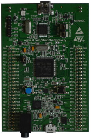
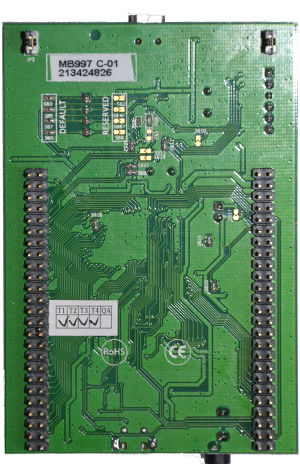
This page is for the STM32F4 Discovery board with STM32F407VGT6, STM32F4 Disco is a familiar board with STM32F401VCT6, do not use this Files for the Disco board !
Overview
- STMicroelectronics STM32F4VGT6 Cortex M4 MCU, up to 168Mhz with floating point unit (FPU), 192 KB RAM, 1024 KB Flash
- on-board STLinkv2 with SWD header (capable of programming onboard or external MCU)
- on-board power regulator for the MCU (3V or 5V Input)
- 1 x user push button
- 4(5) x LED (orange, green, red, blue, green)
- 4(6) x UART (UART1, UART2, UART3, (UART4, UART5), UART6)
- 1(3) x SPI (SPI1, (SPI2, SPI3))
- 2(3) x I2C (I2C1, I2C2, (I2C3))
- 6 x ADC inputs (one is used for BAT voltage)
- 1 x PPM input
- 1 x Spektrum input (with bind pin)
- 97 x 66 mm PCB
- 4 x status LED (USB red, USB green, power, USB OTG green, USB OTG red)
- LIS302DL MEMS 3 axis accelerometer on SPI1
Pinout
The Discovery has a male 100 pin (2x25pin on both sides, also accessible on both sides of the pcb) pinout.
| Pin # | Name | Type | Description | Color |
|---|---|---|---|---|
| PD13 | LED_3 | Out | above LIS302DL | Orange |
| PD12 | LED_4 | Out | left of LIS302DL | Green |
| PD14 | LED_5 | Out | right of LIS302DL | Red |
| PD15 | LED_6 | Out | below LIS302DL | Blue |
| PA9 | LED_9 | Out | same as USB power (VBUS, needs to be enabled in header file) | Green |
| Pin # | Name | Type | Description |
|---|---|---|---|
| PB6 | UART1 TX | Out | UART1 Serial Output, 4k7 pullup for I2C |
| PB7 | UART1 RX | In | UART1 Serial Input |
| Pin # | Name | Type | Description |
|---|---|---|---|
| PD5 | UART2 TX | Out | UART2 Serial Output (usb otg power management fault output open drain) |
| PD6 | UART2 RX | In | UART2 Serial Input, also used for Spektrum input |
| Pin # | Name | Type | Description |
|---|---|---|---|
| PD8 | UART3 TX | Out | UART3 Serial Output |
| PD9 | UART3 RX | In | UART3 Serial Input |
| Pin # | Name | Type | Description |
|---|---|---|---|
| PC10 | UART4 TX | Out | UART4 Serial Output |
| PC11 | UART4 RX | In | UART4 Serial Input |
| Pin # | Name | Type | Description |
|---|---|---|---|
| PC12 | UART5 TX | Out | UART5 Serial Output |
| PD2 | UART5 RX | In | UART5 Serial Input |
| Pin # | Name | Type | Description |
|---|---|---|---|
| PC6 | UART6 TX | Out | UART6 Serial Output |
| PC7 | UART6 RX | In | UART6 Serial Input |
| Pin # | Name | Type | Description |
|---|---|---|---|
| PA5 | SPI1 SCK | I/O | SPI1 Serial clock |
| PA6 | SPI1 MISO | I/O | SPI1 Master In Slave Out |
| PA7 | SPI1 MOSI | I/O | SPI1 Master Out Slave In |
| PE3 | SPI SS2 | I/O | SPI1 Select Slave2 |
| Pin # | Name | Type | Description |
|---|---|---|---|
| PB3 | SPI1 SCK | I/O | SPI1 Serial clock |
| PB4 | SPI1 MISO | I/O | SPI1 Master In Slave Out |
| PB5 | SPI1 MOSI | I/O | SPI1 Master Out Slave In |
| PE2 | SPI SS0 | I/O | SPI1 Select Slave0 |
| Pin # | Name | Type | Description |
|---|---|---|---|
| PB13 | SPI2 SCK | I/O | SPI2 Serial clock |
| PB14 | SPI2 MISO | I/O | SPI2 Master In Slave Out |
| PB15 | SPI2 MOSI | I/O | SPI2 Master Out Slave In |
| PE7 | SPI SS1 | I/O | SPI2 Select Slave1 |
| Pin # | Name | Type | Description |
|---|---|---|---|
| PC10 | SPI3 SCK | I/O | SPI3 Serial clock |
| PC11 | SPI3 MISO | I/O | SPI3 Master In Slave Out |
| PC12 | SPI3 MOSI | I/O | SPI3 Master Out Slave In |
| PE3 | SPI SS2 | I/O | SPI3 Select Slave2 (also used for LIS302DL (SPI1) Slave Select) |
| Pin # | Name | Type | Description |
|---|---|---|---|
| PB8 | I2C1 SCL | I/O | I2C1 Serial Clock |
| PB9 | I2C1 SDA | I/O | I2C1 Serial Data |
| Pin # | Name | Type | Description |
|---|---|---|---|
| PB10 | I2C2 SCL | I/O | I2C2 Serial Clock (also used for MP45DT02 MEMS MIC clock in) |
| PB11 | I2C2 SDA | I/O | I2C2 Serial Data |
| Pin # | Name | Type | Description |
|---|---|---|---|
| PA8 | I2C3 SCL | I/O | I2C3 Serial Clock |
| PC9 | I2C3 SDA | I/O | I2C3 Serial Data |
Note: is disabled in header file, PA8 is used as Spektrum bind pin, PC9 is used as PPM (not Spektrum) input
| Pin # | Name | Type | Description |
|---|---|---|---|
| PB1 | AUX1 | I/O | ADC_1 |
| PC5 | AUX2 | I/O | ADC_2 |
| PC4 | AUX3 | I/O | ADC_3 |
| PA4 | AUX4/BAT | I/O | ADC_4, is used for BAT voltage |
| PC1 | AUX5 | I/O | ADC_5 |
| PC2 | AUX6 | I/O | ADC_6 |
| Pin # | Name | Type | Description |
|---|---|---|---|
| PE9 | PWM0 | Out | Servo 1 |
| PE11 | PWM1 | Out | Servo 2 |
| PE13 | PWM2 | Out | Servo 3 |
| PE14 | PWM3 | Out | Servo 4 |
| PE5 | PWM4 | Out | Servo 5 |
| PE6 | PWM5 | Out | Servo 6 |
| PA3 | PWM6 | Out | Servo 7 |
| PA2 | PWM7 | Out | Servo 8 |
| PA1 | PWM8 | Out | Servo 9 |
| PA0 | PWM9 | Out | Servo 10 |
| PB14 | PWM10 | Out | Servo 11, Can not be used if SPI2 is active |
| PB15 | PWM11 | Out | Servo 12, Can not be used if SPI2 is active |
| Pin # | Name | Type | Description |
|---|---|---|---|
| PC9 | PPM | In | PPM input (remember, you need 100 Ohm serial termination in order to use this) |
| Pin # | Name | Type | Description |
|---|---|---|---|
| PA8 | Bind | Out | Spektrum bind pin |
| PA10 | PPM | IN | Spektrum PPM in |
Jumper
| Pin # | Name | Type | Description |
|---|---|---|---|
| JP1 | JP1 | Switch | MCU Current can be measured here |
| CN3 | CN3 | Switch | closed: STLinkV2 is connected to onboard MCU, open: is not connectec to onboard, only external header |
| Pin # | Name | Type | Description |
|---|---|---|---|
| SB17 | SB17 | Switch | Bypass for JP1, close this for security ! (if JP1 gets loose there is no power supply for the mcu) |
Daughterboard
Currently we have two different breakout/baughter boards.
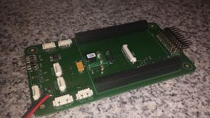
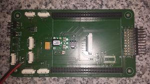
SMD & Molex
Another option with Molex connectors, levelshifters for I2C and SPI, as well as connectors for Spektrum satellites and a can phy would be:
Currently under testing, eagle files are coming, when its completely finished and airworthy :-)
THT
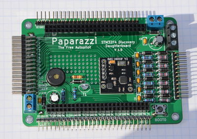
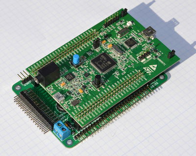
Target for this board is to be a ultra low cost THT daughterboard which should provide as many functions as possible. Also it should be as simple as possible (hence no SMD Components were used).
Notes
- Tall screw terminals can touch the THT solder joints from the discovery board. No electrical but a mechanical contact can appear. Don't force both pcb's all the way together (leave a small gap).
- Only mount the components needed.
- If IR_Sensors are used used, maybe the diodes shouldn't be mounted and the voltage divider should be changed.
- If you use the 22k/2.2k voltage divider for the BAT input, you need to change the VoltageOfAdc see Airframe_Configuration#Battery.
Servo Power options
- External power source (to power servos with a higher voltage or an other voltage regulator, only GND stays connected).
- Power servos from the 5V rail, solder the two solder bridges near the three row header.
The servo rail also powers the RC receiver directly (PPM and Spektrum), take care of that if this rail runs on a higher voltage than 5V!
Servo and 5V net share the same GND!
IMU mounting options
- Drotek 10 DOF can be soldered on the appropriate footprint. (phi, theta and psi need to be 180 degree offset)
- Other IMUs (e.g. MPU6050 breakout) can be soldered on the prototyling area. Use wires to connect it to the Droteks I2C2 pins e.g..
- Mount IMU elsewhere and connect it with cables.
BAT voltage
If you use the 22k/2.2k Resistor divider, you will need to redefine the values for the ADC conversation.
| File: conf/airframes/myplane.xml |
  <section name="BAT">
    ...
    <define name="VOLTAGE_ADC_SCALE" value="0.008864469"/> <!-- R1 (Bat - ADC input) = 22k, R2 (ADC input - GND) = 2.2K--->
    <define name="VOLTAGE_OFFSET" value="0" unit="V"/>
    <define name="VoltageOfAdc(adc)" value="(VOLTAGE_ADC_SCALE * adc + VOLTAGE_OFFSET)"/>
  </section>
|
Also see Airframe_Configuration#Battery.
Firmware Flashing
FLASH_MODE=STLINK is set as default
STM32F4 Discovery can mainly be programmed in two different ways:
STLINK
- with onboard STLinkV2 over SWD
- required hardware: usb to mini USB cable
- required software: st_flash and st_util from Texane
- more information: STLink page
DFU-UTIL
- with the MCU native (embedded in rom) DFU USB bootloader over the micro USB AB connector
- required hardware: USB to micro and USB to mini usb cable
- required external software: dfu-util
- push MCU in DFU mode: connect mini(for power) and micro USB to PC, connect pin BOOT0 with 3V, press reset button(LED LD7 should light up now), disconnect BOOT0
- more information: DFU page
Supplier
THe STM discovery boards look all quite alike. To make sure you get the right board here a direct [link at Farnell] Whatever supplier yo choose make sure it is a STM32F407 ,mind the 07 in the end, board.
