Difference between revisions of "Eagle Tips"
AutumnLeaves (talk | contribs) |
|||
| (3 intermediate revisions by 2 users not shown) | |||
| Line 1: | Line 1: | ||
The [http://www. | The [http://www.cadsoftusa.com Eagle] CAD drawings and schematics are available from the [[Downloads]] page. A freeware version of Eagle program is available for Linux or Windows that allows for viewing and printing the hardware files. | ||
== Printing Schematics == | == Printing Schematics == | ||
Paparazzi schematics were drawn to print on an A4 sheet which is 210mm x 297mm (8.26in x 11.7in). North America uses the Letter size of 8.5in x 11in and will print fine onto two Letter sheets but it is more convenient to print onto a single Letter sized sheet. Below are instructions to do this. | Paparazzi schematics were drawn to print on an A4 sheet which is 210mm x 297mm (8.26in x 11.7in). North America uses the Letter size of 8.5in x 11in and will print fine onto two Letter sheets but it is more convenient to print onto a single Letter sized sheet. Below are instructions for how to do this. | ||
'''From Windows:''' | '''From Windows:''' | ||
With the schematic open go to File -> Print and you will see the print dialog | With the schematic open go to File -> Print and you will see the print dialog | ||
| Line 22: | Line 22: | ||
== Panels == | == Panels == | ||
[[Image:panel.jpg|thumb|Example panel]] | [[Image:panel.jpg|thumb|Example panel]] | ||
If you're going to have PCBs manufactured, you'll probably want to fit several boards on a sheet. This is called a panel. The paparazzi3/hw/panel directory contains a makefile and some config files that will allow you to do that. It uses the [http://claymore.engineer.gvsu.edu/~steriana/Python/gerbmerge/ | If you're going to have PCBs manufactured, you'll probably want to fit several boards on a sheet. This is called a panel. The paparazzi3/hw/panel directory contains a makefile and some config files that will allow you to do that. It uses the [http://claymore.engineer.gvsu.edu/~steriana/Python/gerbmerge/ gerbmerge] program. See how to install on ubuntu [http://blog.bhargavaz.us/2009/05/installing-gerbmerge-on-ubuntu-linux.html gerbmerge install]. The [http://gerbv.sourceforge.net/ gerbv] program will allow you to check your results. | ||
After completing the ''layout.cfg'' and ''layout.def'' files in the panel directory, all you have to do is type ''make _panel''. Then, to view the result, ''make _view'' | After completing the ''layout.cfg'' and ''layout.def'' files in the panel directory, all you have to do is type ''make _panel''. Then, to view the result, ''make _view'' | ||
Latest revision as of 14:38, 17 January 2016
The Eagle CAD drawings and schematics are available from the Downloads page. A freeware version of Eagle program is available for Linux or Windows that allows for viewing and printing the hardware files.
Printing Schematics
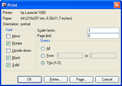
Paparazzi schematics were drawn to print on an A4 sheet which is 210mm x 297mm (8.26in x 11.7in). North America uses the Letter size of 8.5in x 11in and will print fine onto two Letter sheets but it is more convenient to print onto a single Letter sized sheet. Below are instructions for how to do this. From Windows: With the schematic open go to File -> Print and you will see the print dialog
Under STYLE, check off ROTATE, BLACK, and SOLID
Scale Factor is the important setting and you will want to put 0.65. If it cuts too much off, try lowering this number by 0.1 each time.
Under sheets check off select all to print all of the schematic pages 'or' select This to print the schematic page you were currently looking at.
Gerbers
The format generally accepted by PCB manufacturers is called gerber and is a collection of individual files representing each layer or aspect of the PCB. The gerber files can be produced using the CAM processor of Eagle. The commands needed for this operation in Linux are contained in the Makefile of the hw directory, and thus typing make gerber from this directory will produce a set of gerbers.
The Makefile can also be used to get the CAM processor to generate printable documents for the schematics and implantation of parts (pdf and postcript) . Typing make printable in the hw directory should do the trick.
Panels
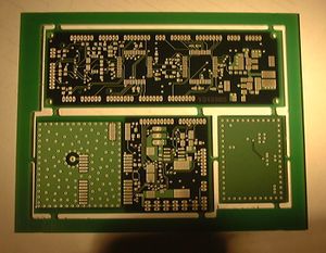
If you're going to have PCBs manufactured, you'll probably want to fit several boards on a sheet. This is called a panel. The paparazzi3/hw/panel directory contains a makefile and some config files that will allow you to do that. It uses the gerbmerge program. See how to install on ubuntu gerbmerge install. The gerbv program will allow you to check your results.
After completing the layout.cfg and layout.def files in the panel directory, all you have to do is type make _panel. Then, to view the result, make _view
3D views
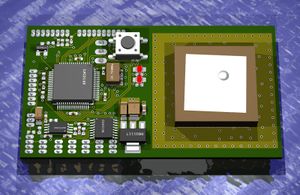
3-D renderings can be produced using the eagle3d script and the povray raytracer. A copy of this script and associated povray libraries are in the paparazzi3/hw/ulp and paparazzi/hw/povray.
To produce such a view from the eagle board view click the ulp button and select the paparazzi3/hw/ulp/3d41.ulp script. The script will produce a file usable by povray. Have the script put the generated file in the paparazzi3/hw/povray directory. Then in this directory, issue the following command povray tiny.pov to have povray generate the image.


