!! WARNING !!
THIS IS A PRELIMINARY DESIGN, IT HAS NOT BEEN TESTED YET.
DO NOT USE FOR MASS PRODUCTION AS LONG AS THIS MESSAGE REMAIN.


Hardware Revision History
| Version # |
Release Date |
Release Notes
|
| v1.00 |
04/2008 |
Initial release of Twog v1
|
Features
- Single LPC2148 MCU
- 8 x Analog input channels 0V - 3.3V (2 channels with optional on-board resistor bridge)
- 1 x 3.3V TTL UART (5V tolerant)
- 8 x PWM outputs
- 1 x R/C receiver PPM frame input
- 1 x SPI bus
- 1 x I2C bus
- 1 x USB (client)
- 5V/2.5A switching power supply & 3.3V/1A linear regulator
- 3 x status LEDs with attached test point
- ?? grams
- 40.2 x 30.5mm (1.6" x 1.2")
- 2 layers PCB design, 0603 components
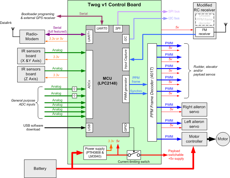
Architecture

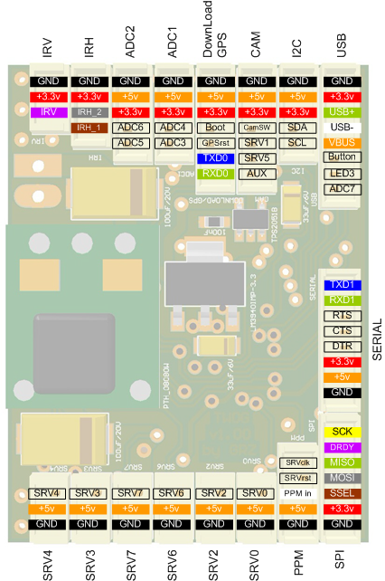
Pinout
Pins Name and Type are specified with respect to the Autopilot Board

SERIAL
| Pin # |
Name |
Type |
Description |
Suggested Color
|
| 1 |
GND |
PWR |
common ground |
Black
|
| 2 |
+5V |
PWR |
5V Rail from Tiny |
Orange
|
| 3 |
+3.3V |
PWR |
3.3V Rail from Tiny |
Red
|
| 4 |
DTR |
|
|
|
| 5 |
CTS |
|
|
|
| 6 |
RTS |
|
|
|
| 7 |
RXD1 |
IN |
UART1 Serial Input (3.3V level, 5V Tolerant) |
Green
|
| 8 |
TXD1 |
OUT |
UART1 Serial Output (3.3V level) |
Blue
|
SPI
| Pin # |
Name |
Type |
Description |
Suggested Color
|
| 1 |
GND |
PWR |
common ground |
Black
|
| 2 |
+3.3V |
PWR |
3.3V Rail from Tiny |
Red
|
| 3 |
SSEL |
IN |
SSP Slave Select. Selects the SSP interface as a slave (SSEL1) |
Brown
|
| 4 |
MOSI |
I/O |
SPI1 Master Out Slave In. Data output from master or data input to slave |
Grey
|
| 5 |
MISO |
I/O |
SPI1 Master In Slave Out. Data input to master or data output from slave |
Green
|
| 6 |
DRDY |
IN |
External interrupt 0 input (EINT0) |
Purple
|
| 7 |
SCK |
I/O |
SPI0 Serial clock. Clock output from master or input to slave |
Yellow
|
PPM
| Pin # |
Name |
Type |
Description |
Suggested Color
|
| 1 |
GND |
PWR |
common ground |
Black
|
| 2 |
+5v |
PWR |
5V Rail from Tiny to R/C receiver supply |
Orange
|
| 3 |
PPM_IN |
IN |
PPM Stream from R/C Receiver (5V tolerant) |
White
|
| 4 |
SERV_RST |
OUT |
external PPM decoder reset (Note 1) |
|
| 5 |
SERV_CLK |
OUT |
external PPM decoder clock (Note 1) |
|
Note 1 : Used only if servos are connected to the R/C receiver
USB
| Pin # |
Name |
Type |
Description |
Suggested Color
|
| 1 |
GND |
PWR |
common ground |
Black
|
| 2 |
+3.3V |
PWR |
3.3V Rail from Tiny |
Red
|
| 3 |
USB+ |
I/O |
USB bidirectional D+ line |
Green
|
| 4 |
USB- |
I/O |
USB bidirectional D- line |
White
|
| 5 |
VBUS |
IN |
Indicates the presence of USB bus power (P0.23) (5V level) |
Orange
|
| 6 |
BUTTON |
IN |
External Button (+3.3v pullup) |
|
| 7 |
LED3 |
OUT |
GPIO (LED #3 command) |
|
| 8 |
ADC_7 |
IN |
Analog to Digital Converter Input #7 |
|
IRV
| Pin # |
Name |
Type |
Description |
Suggested Color
|
| 1 |
GND |
PWR |
common ground |
Black
|
| 2 |
+3.3V |
PWR |
3.3V Rail from Tiny |
Red
|
| 3 |
IRV |
IN |
Vertical IR Sensor signal (Analog to Digital Converter Input #0) |
Purple
|
IRH
| Pin # |
Name |
Type |
Description |
Suggested Color
|
| 1 |
GND |
PWR |
common ground |
Black
|
| 2 |
+3.3V |
PWR |
3.3V Rail from Tiny |
Red
|
| 3 |
IRH_2 |
IN |
Horizontal IR Sensor signal axis 2 (Analog to Digital Converter Input #2) |
Grey
|
| 4 |
IRH_1 |
IN |
Horizontal IR Sensor signal axis 1 (Analog to Digital Converter Input #1) |
Brown
|
ADC1
| Pin # |
Name |
Type |
Description |
Suggested Color
|
| 1 |
GND |
PWR |
common ground |
Black
|
| 2 |
+5v |
PWR |
5V Rail from Tiny |
Orange
|
| 3 |
+3.3V |
PWR |
3.3V Rail from Tiny |
Red
|
| 4 |
ADC_4 |
IN |
Analog to Digital Converter Input #4 |
|
| 5 |
ADC_3 |
IN |
Analog to Digital Converter Input #3 |
|
ADC2
| Pin # |
Name |
Type |
Description |
Suggested Color
|
| 1 |
GND |
PWR |
common ground |
Black
|
| 2 |
+5v |
PWR |
5V Rail from Tiny |
Orange
|
| 3 |
+3.3V |
PWR |
3.3V Rail from Tiny |
Red
|
| 4 |
ADC_6 |
IN |
Analog to Digital Converter Input #6 (Maximum input level can be selected with R12 value) |
|
| 5 |
ADC_5 |
IN |
Analog to Digital Converter Input #5 (Maximum input level can be selected with R13 value) |
|
DOWNLOAD/GPS
| Pin # |
Name |
Type |
Description |
Suggested Color
|
| 1 |
GND |
PWR |
common ground |
Black
|
| 2 |
+5v |
PWR |
5V Rail from Tiny |
Orange
|
| 3 |
+3.3V |
PWR |
3.3V Rail from Tiny |
Red
|
| 4 |
BOOT |
IN |
In-Circuit Serial Programming (ISP) enable (P0.14, +3.3v pullup) (Note 2) |
|
| 5 |
GPS_RESET |
IN |
leave unconnected, hold this pin low only for bootloader programming |
|
| 6 |
TXD0 |
OUT |
UART0 Serial Output (usable with an external GPS receiver) |
Blue
|
| 7 |
RXD0 |
IN |
UART0 Serial Input (usable with an external GPS receiver) |
Green
|
Note 2 : Holding this pin low for at least 3mS after a RESET (or power up) instructs the controller to enter programming mode.
I2C
| Pin # |
Name |
Type |
Description |
Suggested Color
|
| 1 |
GND |
PWR |
common ground |
Black
|
| 2 |
+5V |
PWR |
5V Rail from Tiny |
Orange
|
| 3 |
+3.3V |
PWR |
3.3V Rail from Tiny |
Red
|
| 4 |
SDA |
I/O |
I2C bus Serial DAta |
|
| 5 |
SCL |
I/O |
I2C bus Serial CLock |
|
CAM
| Pin # |
Name |
Type |
Description |
Suggested Color
|
| 1 |
GND |
PWR |
common ground |
Black
|
| 2 |
+5V |
PWR |
5V Rail from Tiny |
Orange
|
| 3 |
+3.3V |
PWR |
3.3V Rail from Tiny |
Red
|
| 4 |
CAM_SW |
OUT |
video source/payload selection signal |
|
| 5 |
SRV_1 |
OUT |
Servo PWM signal #1 |
|
| 6 |
SRV_5 |
OUT |
Servo PWM signal #5 |
|
| 7 |
AUX |
PWR |
video/payload switchable 5V power suply |
|
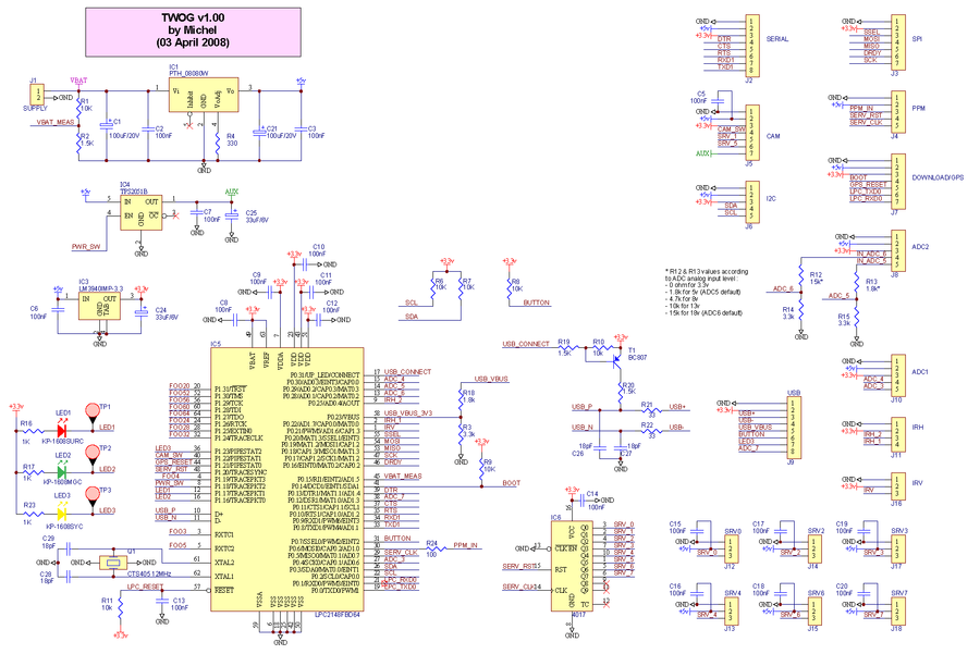
Schematic
PCB
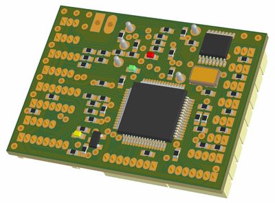
PCB top side view (Olimex)
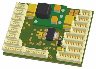
PCB bottom side view (Olimex)
Gerber & Drill Files
Download Twog v1.00 gerber & drill files (zip)
RS274X, units = Inches, format = 2:5
- Twog_v1-00.GTO (Top Component Print Layer)
- Twog_v1-00.GTS (Top Solder Mask)
- Twog_v1-00.GTL (Top Copper Layer)
- Twog_v1-00.GBL (Bottom Copper Layer)
- Twog_v1-00.GBS (Bottom Solder Mask)
- Twog_v1-00.DRI (NC XY coordinates & Drill tools sizes)
Possible PCB Manufacturers
Assembly
Components Layout
Bottom components details
Bill Of Material
Download Twog v1.00 Bill Of Material (zipped .xls file)
| Qty |
Manufacturer part # |
Schematic part name / value |
Designator |
Description |
Manufacturer |
Package |
Optional |
Digikey.com |
Other distributor
|
| Resistors
|
| 2 |
ERJ-3EKF33R0V |
33 |
R21, R22 |
1/16W, 5% |
Panasonic |
0603 |
|
P33HCT-ND |
|
| 1 |
ERJ-3EKF1000V |
100 |
R24 |
1/16W, 5% |
Panasonic |
0603 |
|
P100HCT-ND |
|
| 1 |
ERJ-3EKF3300V |
330 |
R4 |
1/16W, 5% |
Panasonic |
0603 |
|
P330HCT-ND |
|
| 3 |
ERJ-3EKF1001V |
1K |
R16, R17, R23 |
1/16W, 5% |
Panasonic |
0603 |
|
P1.00KHCT-ND |
|
| 3 |
ERJ-3EKF1501V |
1.5K |
R2, R19, R20 |
1/16W, 5% |
Panasoni |
0603 |
|
P1.50KHCT-ND |
|
| 2 |
ERJ-3EKF1801V |
1.8k (see note1) |
R13,R18 |
1/16W, 5% |
Panasonic |
0603 |
|
P1.8KHCT-ND |
|
| 3 |
ERJ-3EKF3301V |
3.3K |
R3, R14, R15 |
1/16W, 5% |
Panasonic |
0603 |
|
P3.3KHCT-ND |
|
| 7 |
ERJ-3EKF1002V |
10K |
R1, R6 to R11 |
1/16W, 5% |
Panasonic |
0603 |
|
P10.0KHCT-ND |
|
| 1 |
ERJ-3EKF1502V |
15K (see note2) |
R12 |
1/16W, 5% |
Panasonic |
0603 |
|
P15.0KHCT-ND |
|
| Capacitors
|
| 4 |
C0603C180J5GAC |
18pF |
C26 to C29 |
50V, 5% |
Kemet |
0603 |
|
399-1052-1-ND |
|
| 18 |
C0603C104K5RAC |
100nF |
C2,C3,C5 to C20 |
50V, 10% |
Kemet |
0603 |
|
399-5089-1-ND |
|
| 2 |
T520A336M006ATE070 |
33uF/6V |
C24, C25 |
SMD tantalum capacitor |
Kemet |
A case (EIA 3216-18) |
|
399-4719-1-ND |
|
| 2 |
TAJD107K020R |
100uF/20V |
C1, C21 |
SMD tantalum capacitor |
AVX Corp. |
D case (EIA 7343-31) |
|
478-1724-1-ND |
|
| Semiconductors
|
| 1 |
LM3940IMP-3.3 |
LM3940IMP-3.3 |
IC3 |
1A low dropout regulator for 5V to 3.3V conversion |
National Semic. |
SOT223 |
|
LM3940IMP-3.3CT-ND |
|
| 1 |
TPS2051BDBV |
TPS2051B |
IC4 |
Current Limited Power Distribution Switch |
Texas Instr. |
SOT23-5 |
yes |
296-21265-1-ND |
|
| 1 |
LPC2148FBD64 |
LPC2148FBD64 |
IC5 |
Single-chip ARM7 32-bit microcontroller |
NXP |
LQFP64 |
|
568-1765-ND |
|
| 1 |
CD4017BPW |
4017 |
IC6 |
Decade Counter/Divider with 10 Decoded Outputs |
Texas Instr. |
TSSOP16 |
|
296-14252-1-ND |
|
| 1 |
APT1608SURCK |
KP-1608SURC |
LED1 |
SMD Chip Red LED Lamp |
Kingbright |
0603 |
yes |
754-1123-1-ND |
|
| 1 |
APT1608MGC |
KP-1608MGC |
LED2 |
SMD Chip Green LED Lamp |
Kingbright |
0603 |
|
754-1118-1-ND |
|
| 1 |
APT1608SYCK |
KP-1608SYC |
LED3 |
SMD Chip Yellow LED Lamp |
Kingbright |
0603 |
yes |
754-1124-1-ND |
|
| 1 |
BC807-40 |
BC807 |
T1 |
PNP general purpose transistor |
NXP |
SOT23 |
|
568-1629-1-ND |
|
| Modules
|
| 1 |
PTH08080WAH |
PTH_08080W |
IC1 |
2.25A Wide-input adjustable switching regulator |
Texas Instr. |
specific |
|
296-20432-ND |
|
| Connectors
|
| 7 |
53047-0310 |
SRV0, SRV4, SRV2, SRV6, IRV, SRV3, SRV7 |
J12 to J18 |
Picoblade 3 pins 1.25mm straight header |
Molex |
specific |
|
WM1732-ND |
|
| 1 |
53047-0410 |
IRH |
J11 |
Picoblade 4 pins 1.25mm straight header |
Molex |
specific |
|
WM1733-ND |
|
| 4 |
53047-0510 |
PPM,I2C,ADC2,ADC1 |
J4, J6, J8, J10 |
Picoblade 5 pins 1.25mm straight header |
Molex |
specific |
J6,J8,J10 |
WM1734-ND |
|
| 3 |
53047-0710 |
SPI,CAM,DOWNLOAD/GPS |
J3, J5, J7 |
Picoblade 7 pins 1.25mm straight header |
Molex |
specific |
J3,J5 |
WM1736-ND |
|
| 2 |
53047-0810 |
SERIAL,USB |
J2, J9 |
Picoblade 8 pins 1.25mm straight header |
Molex |
specific |
|
WM1737-ND |
|
| Other
|
| 1 |
405C35B12M00000 |
CTS405 12MHz |
Q1 |
SMD 12MHz Quartz Crystal |
CTS |
specific |
|
CTX639CT-ND |
|
Downloads
Source files
Gerber & Drill files
Assembly files
