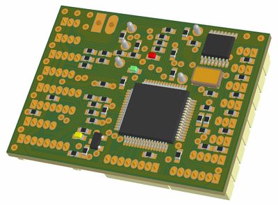
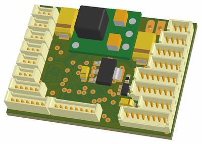
Twog v1
Jump to navigation
Jump to search
!! WARNING !!
THIS IS A PRELIMINARY DESIGN, IT HAS NOT BEEN TESTED YET.
DO NOT USE FOR MASS PRODUCTION AS LONG AS THIS MESSAGE REMAIN.
Hardware Revision History
| Version # | Release Date | Release Notes |
|---|---|---|
| v1.00 | 04/2008 | Initial release of Twog v1 |
Features
- Single LPC2148 MCU
- 8 x Analog input channels 0V - 3.3V (2 channels with optional on-board resistor bridge)
- 1 x 3.3V TTL UART (5V tolerant)
- 8 x PWM outputs
- 1 x R/C receiver PPM frame input
- 1 x SPI bus
- 1 x I2C bus
- 1 x USB (client)
- 5V/2.5A switching power supply & 3.3V/1A linear regulator
- 3 x status LEDs with attached test point
- ?? grams
- 40.2 x 30.5mm (1.6" x 1.2")
- 2 layers PCB design, 0603 components
Architecture
under construction
Pinout
under construction
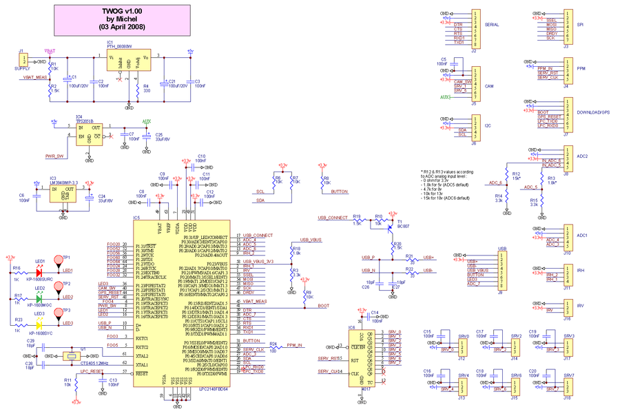
Schematic
PCB
Gerber & Drill Files
Download Twog v1.00 gerber & drill files (zip)
RS274X, units = Inches, format = 2:5
- Twog_v1-00.GTO (Top Component Print Layer)
- Twog_v1-00.GTS (Top Solder Mask)
- Twog_v1-00.GTL (Top Copper Layer)
- Twog_v1-00.GBL (Bottom Copper Layer)
- Twog_v1-00.GBS (Bottom Solder Mask)
- Twog_v1-00.DRI (NC XY coordinates & Drill tools sizes)
Possible PCB Manufacturers
Assembly
Components Layout
Bill Of Material
Download Twog v1.00 Bill Of Material (zipped .xls file)
Downloads
Source files
Gerber & Drill files
Assembly files


