Difference between revisions of "Twog v1"
Jump to navigation
Jump to search
| Line 1: | Line 1: | ||
[[Image:Twog_v1-00_3D_top.jpg|400px|Twog v1.00 3D top view]] | [[Image:Twog_v1-00_3D_top.jpg|400px|Twog v1.00 3D top view]] | ||
[[Image:Twog_v1-00_3D_bottom.jpg|400px|Twog v1.00 3D bottom view]] | [[Image:Twog_v1-00_3D_bottom.jpg|400px|Twog v1.00 3D bottom view]] | ||
Revision as of 23:54, 10 June 2008


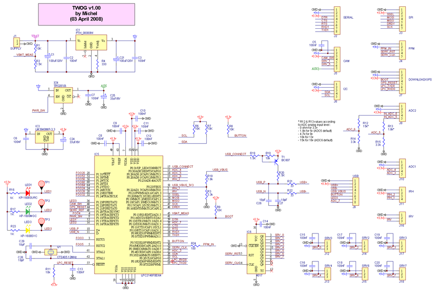
Hardware Revision History
| Version # | Release Date | Release Notes |
|---|---|---|
| v1.00 | 04/2008 | Initial release of Twog v1 |
Features
- Single LPC2148 MCU
- 8 x Analog input channels 0V - 3.3V (2 channels with optional on-board resistor bridge)
- 1 x 3.3V TTL UART (5V tolerant)
- 8 x PWM outputs
- 1 x R/C receiver PPM frame input
- 1 x SPI bus
- 1 x I2C bus
- 1 x USB (client)
- 5V/2.5A switching power supply & 3.3V/1A linear regulator
- 3 x status LEDs with attached test point
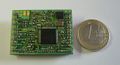
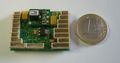
- 8 grams (0.28 oz)
- 40.2 x 30.5mm (1.6" x 1.2")
- 2 layers PCB design, 0603 components
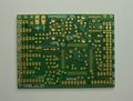
Top side
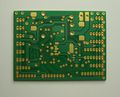
Bottom side
Top side
Bottom side


Architecture

Pinout
Pins Name and Type are specified with respect to the Autopilot Board

| Pin # | Name | Type | Description | Suggested Color |
|---|---|---|---|---|
| 1 | GND | PWR | common ground | Black |
| 2 | +5V | PWR | 5V Rail from Tiny | Orange |
| 3 | +3.3V | PWR | 3.3V Rail from Tiny | Red |
| 4 | DTR | |||
| 5 | CTS | |||
| 6 | RTS | |||
| 7 | RXD1 | IN | UART1 Serial Input (3.3V level, 5V Tolerant) | Green |
| 8 | TXD1 | OUT | UART1 Serial Output (3.3V level) | Blue |
| Pin # | Name | Type | Description | Suggested Color |
|---|---|---|---|---|
| 1 | GND | PWR | common ground | Black |
| 2 | +3.3V | PWR | 3.3V Rail from Tiny | Red |
| 3 | SSEL | IN | SSP Slave Select. Selects the SSP interface as a slave (SSEL1) | Brown |
| 4 | MOSI | I/O | SPI1 Master Out Slave In. Data output from master or data input to slave | Grey |
| 5 | MISO | I/O | SPI1 Master In Slave Out. Data input to master or data output from slave | Green |
| 6 | DRDY | IN | External interrupt 0 input (EINT0) | Purple |
| 7 | SCK | I/O | SPI0 Serial clock. Clock output from master or input to slave | Yellow |
| Pin # | Name | Type | Description | Suggested Color |
|---|---|---|---|---|
| 1 | GND | PWR | common ground | Black |
| 2 | +5v | PWR | 5V Rail from Tiny to R/C receiver supply | Orange |
| 3 | PPM_IN | IN | PPM Stream from R/C Receiver (5V tolerant) | White |
| 4 | SERV_RST | OUT | external PPM decoder reset (Note 1) | |
| 5 | SERV_CLK | OUT | external PPM decoder clock (Note 1) |
Note 1 : Used only if servos are connected to the R/C receiver
| Pin # | Name | Type | Description | Suggested Color |
|---|---|---|---|---|
| 1 | GND | PWR | common ground | Black |
| 2 | +3.3V | PWR | 3.3V Rail from Tiny | Red |
| 3 | USB+ | I/O | USB bidirectional D+ line | Green |
| 4 | USB- | I/O | USB bidirectional D- line | White |
| 5 | VBUS | IN | Indicates the presence of USB bus power (P0.23) (5V level) | Orange |
| 6 | BUTTON | IN | External Button (+3.3v pullup) | |
| 7 | LED3 | OUT | GPIO (LED #3 command) | |
| 8 | ADC_7 | IN | Analog to Digital Converter Input #7 |
| Pin # | Name | Type | Description | Suggested Color |
|---|---|---|---|---|
| 1 | GND | PWR | common ground | Black |
| 2 | +3.3V | PWR | 3.3V Rail from Tiny | Red |
| 3 | IRV | IN | Vertical IR Sensor signal (Analog to Digital Converter Input #0) | Purple |
| Pin # | Name | Type | Description | Suggested Color |
|---|---|---|---|---|
| 1 | GND | PWR | common ground | Black |
| 2 | +3.3V | PWR | 3.3V Rail from Tiny | Red |
| 3 | IRH_2 | IN | Horizontal IR Sensor signal axis 2 (Analog to Digital Converter Input #2) | Grey |
| 4 | IRH_1 | IN | Horizontal IR Sensor signal axis 1 (Analog to Digital Converter Input #1) | Brown |
| Pin # | Name | Type | Description | Suggested Color |
|---|---|---|---|---|
| 1 | GND | PWR | common ground | Black |
| 2 | +5v | PWR | 5V Rail from Tiny | Orange |
| 3 | +3.3V | PWR | 3.3V Rail from Tiny | Red |
| 4 | ADC_4 | IN | Analog to Digital Converter Input #4 | |
| 5 | ADC_3 | IN | Analog to Digital Converter Input #3 |
| Pin # | Name | Type | Description | Suggested Color |
|---|---|---|---|---|
| 1 | GND | PWR | common ground | Black |
| 2 | +5v | PWR | 5V Rail from Tiny | Orange |
| 3 | +3.3V | PWR | 3.3V Rail from Tiny | Red |
| 4 | ADC_6 | IN | Analog to Digital Converter Input #6 (Maximum input level can be selected with R12 value) | |
| 5 | ADC_5 | IN | Analog to Digital Converter Input #5 (Maximum input level can be selected with R13 value) |
| Pin # | Name | Type | Description | Suggested Color |
|---|---|---|---|---|
| 1 | GND | PWR | common ground | Black |
| 2 | +5v | PWR | 5V Rail from Tiny | Orange |
| 3 | +3.3V | PWR | 3.3V Rail from Tiny | Red |
| 4 | BOOT | IN | In-Circuit Serial Programming (ISP) enable (P0.14, +3.3v pullup) (Note 2) | |
| 5 | GPS_RESET | IN | leave unconnected, hold this pin low only for bootloader programming | |
| 6 | TXD0 | OUT | UART0 Serial Output (usable with an external GPS receiver) | Blue |
| 7 | RXD0 | IN | UART0 Serial Input (usable with an external GPS receiver) | Green |
Note 2 : Holding this pin low for at least 3mS after a RESET (or power up) instructs the controller to enter programming mode.
| Pin # | Name | Type | Description | Suggested Color |
|---|---|---|---|---|
| 1 | GND | PWR | common ground | Black |
| 2 | +5V | PWR | 5V Rail from Tiny | Orange |
| 3 | +3.3V | PWR | 3.3V Rail from Tiny | Red |
| 4 | SDA | I/O | I2C bus Serial DAta | |
| 5 | SCL | I/O | I2C bus Serial CLock |
| Pin # | Name | Type | Description | Suggested Color |
|---|---|---|---|---|
| 1 | GND | PWR | common ground | Black |
| 2 | +5V | PWR | 5V Rail from Tiny | Orange |
| 3 | +3.3V | PWR | 3.3V Rail from Tiny | Red |
| 4 | CAM_SW | OUT | video source/payload selection signal | |
| 5 | SRV_1 | OUT | Servo PWM signal #1 | |
| 6 | SRV_5 | OUT | Servo PWM signal #5 | |
| 7 | AUX | PWR | video/payload switchable 5V power suply |
Schematic

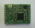
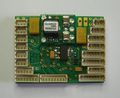
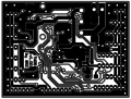
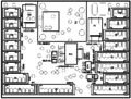
PCB
PCB top side view (Olimex)
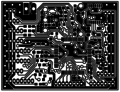
PCB top copper
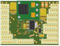
PCB bottom side view (Olimex)
PCB bottom copper


Gerber & Drill Files
Download Twog v1.00 gerber & drill files (zip)
RS274X, units = Inches, format = 2:5
- Twog_v1-00.GTO (Top Component Print Layer)
- Twog_v1-00.GTS (Top Solder Mask)
- Twog_v1-00.GTL (Top Copper Layer)
- Twog_v1-00.GBL (Bottom Copper Layer)
- Twog_v1-00.GBS (Bottom Solder Mask)
- Twog_v1-00.DRI (NC XY coordinates & Drill tools sizes)
Possible PCB Manufacturers
Assembly
Components Layout
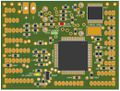
Top components Layout
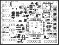
Bottom components Layout
Top components details
Bottom components details


Bill Of Material
Download Twog v1.00 Bill Of Material (zipped .xls file)
| Qty | Manufacturer part # | Schematic part name / value | Designator | Description | Manufacturer | Package | Optional | Digikey.com | Other distributor |
|---|---|---|---|---|---|---|---|---|---|
| Resistors | |||||||||
| 2 | ERJ-3EKF33R0V | 33 | R21, R22 | 1/16W, 5% | Panasonic | 0603 | P33HCT-ND | ||
| 1 | ERJ-3EKF1000V | 100 | R24 | 1/16W, 5% | Panasonic | 0603 | P100HCT-ND | ||
| 1 | ERJ-3EKF3300V | 330 | R4 | 1/16W, 5% | Panasonic | 0603 | P330HCT-ND | ||
| 3 | ERJ-3EKF1001V | 1K | R16, R17, R23 | 1/16W, 5% | Panasonic | 0603 | P1.00KHCT-ND | ||
| 3 | ERJ-3EKF1501V | 1.5K | R2, R19, R20 | 1/16W, 5% | Panasoni | 0603 | P1.50KHCT-ND | ||
| 2 | ERJ-3EKF1801V | 1.8k (see note1) | R13,R18 | 1/16W, 5% | Panasonic | 0603 | P1.8KHCT-ND | ||
| 3 | ERJ-3EKF3301V | 3.3K | R3, R14, R15 | 1/16W, 5% | Panasonic | 0603 | P3.3KHCT-ND | ||
| 7 | ERJ-3EKF1002V | 10K | R1, R6 to R11 | 1/16W, 5% | Panasonic | 0603 | P10.0KHCT-ND | ||
| 1 | ERJ-3EKF1502V | 15K (see note2) | R12 | 1/16W, 5% | Panasonic | 0603 | P15.0KHCT-ND | ||
| Capacitors | |||||||||
| 4 | C0603C180J5GAC | 18pF | C26 to C29 | 50V, 5% | Kemet | 0603 | 399-1052-1-ND | ||
| 18 | C0603C104K5RAC | 100nF | C2,C3,C5 to C20 | 50V, 10% | Kemet | 0603 | 399-5089-1-ND | ||
| 2 | T520A336M006ATE070 | 33uF/6V | C24, C25 | SMD tantalum capacitor | Kemet | A case (EIA 3216-18) | 399-4719-1-ND | ||
| 2 | TAJD107K020R | 100uF/20V | C1, C21 | SMD tantalum capacitor | AVX Corp. | D case (EIA 7343-31) | 478-1724-1-ND | ||
| Semiconductors | |||||||||
| 1 | LM3940IMP-3.3 | LM3940IMP-3.3 | IC3 | 1A low dropout regulator for 5V to 3.3V conversion | National Semic. | SOT223 | LM3940IMP-3.3CT-ND | ||
| 1 | TPS2051BDBV | TPS2051B | IC4 | Current Limited Power Distribution Switch | Texas Instr. | SOT23-5 | yes | 296-21265-1-ND | |
| 1 | LPC2148FBD64 | LPC2148FBD64 | IC5 | Single-chip ARM7 32-bit microcontroller | NXP | LQFP64 | 568-1765-ND | ||
| 1 | CD4017BPW | 4017 | IC6 | Decade Counter/Divider with 10 Decoded Outputs | Texas Instr. | TSSOP16 | 296-14252-1-ND | ||
| 1 | APT1608SURCK | KP-1608SURC | LED1 | SMD Chip Red LED Lamp | Kingbright | 0603 | yes | 754-1123-1-ND | |
| 1 | APT1608MGC | KP-1608MGC | LED2 | SMD Chip Green LED Lamp | Kingbright | 0603 | 754-1118-1-ND | ||
| 1 | APT1608SYCK | KP-1608SYC | LED3 | SMD Chip Yellow LED Lamp | Kingbright | 0603 | yes | 754-1124-1-ND | |
| 1 | BC807-40 | BC807 | T1 | PNP general purpose transistor | NXP | SOT23 | 568-1629-1-ND | ||
| Modules | |||||||||
| 1 | PTH08080WAH | PTH_08080W | IC1 | 2.25A Wide-input adjustable switching regulator | Texas Instr. | specific | 296-20432-ND | ||
| Connectors | |||||||||
| 7 | 53047-0310 | SRV0, SRV4, SRV2, SRV6, IRV, SRV3, SRV7 | J12 to J18 | Picoblade 3 pins 1.25mm straight header | Molex | specific | WM1732-ND | ||
| 1 | 53047-0410 | IRH | J11 | Picoblade 4 pins 1.25mm straight header | Molex | specific | WM1733-ND | ||
| 4 | 53047-0510 | PPM,I2C,ADC2,ADC1 | J4, J6, J8, J10 | Picoblade 5 pins 1.25mm straight header | Molex | specific | J6,J8,J10 | WM1734-ND | |
| 3 | 53047-0710 | SPI,CAM,DOWNLOAD/GPS | J3, J5, J7 | Picoblade 7 pins 1.25mm straight header | Molex | specific | J3,J5 | WM1736-ND | |
| 2 | 53047-0810 | SERIAL,USB | J2, J9 | Picoblade 8 pins 1.25mm straight header | Molex | specific | WM1737-ND | ||
| Other | |||||||||
| 1 | 405C35B12M00000 | CTS405 12MHz | Q1 | SMD 12MHz Quartz Crystal | CTS | specific | CTX639CT-ND | ||
Downloads
Source files
Gerber & Drill files
Assembly files