Tiny v2
Features
- Single LPC2148 MCU
- 8 Analog input channels 0V - 3.3V (2 channels with optional on-board 5v -> 3.3v resistor bridge)
- 1 3.3V TTL UART (5V tolerant)
- 8 PWM outputs
- 1 R/C receiver PPM frame input
- 1 SPI bus
- 1 I2C bus
- 1 USB (client)
- Integrated GPS receiver and patch antenna (4Hz update)
- 5V/2.5A switching power supply & 3.3V/1A linear regulator
- 3 status LEDs with attached test point
- ?? grams
- 70.8 x 40mm (smaller then a banking card)
- 2 layers PCB design, 0603 components
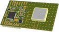
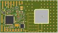
Tiny v2.1 3D top view (18mm GPS antenna)
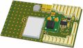
Tiny v2.1 3D bottom view
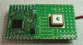
Tiny v2.1 top side view (13mm GPS antenna)
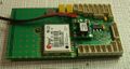
Tiny v2.1 bottom side view


The Tiny v2.1 autopilot uses a single Philips LPC2148 ARM7 based microcontroller. The ARM7 is a low-power 32-bit RISC processor core and the Philips LPC2148 has 512KB on-chip Flash ROM, 40KB RAM and can be clocked at 60MHz.
Although critical control code such as the R/C interface and servo output are well segregated in Paparazzi software and well protected from interference from flaws in the stability/navigation/comm/payload code, great care must be taken when experimenting with new software as some errors can cause a the processor to halt or stall for extended periods causing total loss of control.
Architecture
under construction
Pinout (v2.11)
Pins Name and Type are specified with respect to the Autopilot Board

| Pin # | Name | Type | Description | Suggested Color |
|---|---|---|---|---|
| 1 | GND | PWR | common ground | Black |
| 2 | +5V | PWR | 5V Rail from Tiny | Orange |
| 3 | +3.3V | PWR | 3.3V Rail from Tiny | Red |
| 4 | DTR | |||
| 5 | CTS | |||
| 6 | RTS | |||
| 7 | RXD1 | IN | UART1 Serial Input (3.3V level, 5V Tolerant) | Green |
| 8 | TXD1 | OUT | UART1 Serial Output (3.3V level) | Blue |
| Pin # | Name | Type | Description | Suggested Color |
|---|---|---|---|---|
| 1 | GND | PWR | common ground | Black |
| 2 | +3.3V | PWR | 3.3V Rail from Tiny | Red |
| 3 | SSEL | IN | SSP Slave Select. Selects the SSP interface as a slave (SSEL1) | Braun |
| 4 | MOSI | I/O | SPI1 Master Out Slave In. Data output from master or data input to slave | Grey |
| 5 | MISO | I/O | SPI1 Master In Slave Out. Data input to master or data output from slave | Green |
| 6 | DRDY | IN | External interrupt 0 input (EINT0) | Purple |
| 7 | SCK | I/O | SPI0 Serial clock. Clock output from master or input to slave | Yellow |
| Pin # | Name | Type | Description | Suggested Color |
|---|---|---|---|---|
| 1 | GND | PWR | common ground | Black |
| 2 | +5v | PWR | 5V Rail from Tiny to R/C receiver supply | Orange |
| 3 | PPM_IN | IN | PPM Stream from R/C Receiver (5V tolerant) | White |
| 4 | SERV_RST | OUT | external PPM decoder reset (Note 1) | |
| 5 | SERV_CLK | OUT | external PPM decoder clock (Note 1) |
Note 1 : Used only if servos are connected to the R/C receiver
| Pin # | Name | Type | Description | Suggested Color |
|---|---|---|---|---|
| 1 | GND | PWR | common ground | Black |
| 2 | +3.3V | PWR | 3.3V Rail from Tiny | Red |
| 3 | USB+ | I/O | USB bidirectional D+ line | Green |
| 4 | USB- | I/O | USB bidirectional D- line | White |
| 5 | VBUS | IN | Indicates the presence of USB bus power (P0.23) (5V level) | Orange |
| 6 | BUTTON | IN | External Button (+3.3v pullup) | |
| 7 | LED3 | OUT | GPIO (LED #3 command) | |
| 8 | ADC_7 | IN | Analog to Digital Converter Input #7 |
| Pin # | Name | Type | Description | Suggested Color |
|---|---|---|---|---|
| 1 | GND | PWR | common ground | Black |
| 2 | +3.3V | PWR | 3.3V Rail from Tiny | Red |
| 3 | IRV | IN | Vertical IR Sensor signal (Analog to Digital Converter Input #0) | Purple |
| Pin # | Name | Type | Description | Suggested Color |
|---|---|---|---|---|
| 1 | GND | PWR | common ground | Black |
| 2 | +3.3V | PWR | 3.3V Rail from Tiny | Red |
| 3 | IRH_2 | IN | Horizontal IR Sensor signal axis 2 (Analog to Digital Converter Input #2) | Grey |
| 4 | IRH_1 | IN | Horizontal IR Sensor signal axis 1 (Analog to Digital Converter Input #1) | Braun |
| Pin # | Name | Type | Description | Suggested Color |
|---|---|---|---|---|
| 1 | GND | PWR | common ground | Black |
| 2 | +5v | PWR | 5V Rail from Tiny | Orange |
| 3 | +3.3V | PWR | 3.3V Rail from Tiny | Red |
| 4 | ADC_4 | IN | Analog to Digital Converter Input #4 | |
| 5 | ADC_3 | IN | Analog to Digital Converter Input #3 |
| Pin # | Name | Type | Description | Suggested Color |
|---|---|---|---|---|
| 1 | GND | PWR | common ground | Black |
| 2 | +5v | PWR | 5V Rail from Tiny | Orange |
| 3 | +3.3V | PWR | 3.3V Rail from Tiny | Red |
| 4 | ADC_6 | IN | Analog to Digital Converter Input #6 (Maximum input level can be selected with R12 & R14 values) | |
| 5 | ADC_5 | IN | Analog to Digital Converter Input #5 (Maximum input level can be selected with R13 & R15 values) |
| Pin # | Name | Type | Description | Suggested Color |
|---|---|---|---|---|
| 1 | GND | PWR | common ground | Black |
| 2 | +5v | PWR | 5V Rail from Tiny | Orange |
| 3 | +3.3V | PWR | 3.3V Rail from Tiny | Red |
| 4 | BOOT | IN | In-Circuit Serial Programming (ISP) enable (P0.14, +3.3v pullup) (Note 2) | |
| 5 | GPS_RESET | IN | leave unconnected, hold this pin low only for bootloader programming | |
| 6 | TXD0 | OUT | UART0 Serial Output (shared with GPS receiver) | Blue |
| 7 | RXD0 | IN | UART0 Serial Input (shared with GPS receiver) | Green |
Note 2 : Holding this pin low for at least 3mS after a RESET (or power up) instructs the controller to enter programming mode.
| Pin # | Name | Type | Description | Suggested Color |
|---|---|---|---|---|
| 1 | GND | PWR | common ground | Black |
| 2 | +5V | PWR | 5V Rail from Tiny | Orange |
| 3 | +3.3V | PWR | 3.3V Rail from Tiny | Red |
| 4 | SDA | I/O | I2C bus Serial DAta | |
| 5 | SCL | I/O | I2C bus Serial CLock |
| Pin # | Name | Type | Description | Suggested Color |
|---|---|---|---|---|
| 1 | GND | PWR | common ground | Black |
| 2 | +5V | PWR | 5V Rail from Tiny | Orange |
| 3 | +3.3V | PWR | 3.3V Rail from Tiny | Red |
| 4 | CAM_SW | OUT | video source/payload selection signal | |
| 5 | SRV_1 | OUT | Servo PWM signal #1 | |
| 6 | SRV_5 | OUT | Servo PWM signal #5 | |
| 7 | AUX | PWR | video/payload switchable 5V power suply |
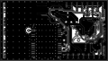
Schematic (v2.11)
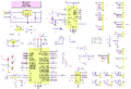
Tiny v2.11 Schematic

PCB (v2.11)
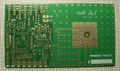
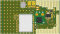
Tiny v2.1 PCB top side view (Olimex)
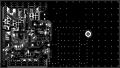
Tiny v2.11 PCB top copper
Tiny v2.1 PCB bottom side view (Olimex)
Tiny v2.11 PCB bottom copper


Gerber & Drill Files (v2.11)
Download Tiny v2.11 gerber & drill files (zip)
RS274X, units = Inches, format = 2:5
- Tiny_v2-11.GTO (Top Component Print Layer)
- Tiny_v2-11.GTS (Top Solder Mask)
- Tiny_v2-11.GTL (Top Copper Layer)
- Tiny_v2-11.GBL (Bottom Copper Layer)
- Tiny_v2-11.GBS (Bottom Solder Mask)
- Tiny_v2-11.DRI (NC XY coordinates & Drill tools sizes)
Possible PCB Manufacturers
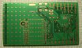
Components Assembly (v2.11)
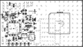
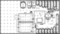
Components Layout
Tiny v2.11 top components Layout
Tiny v2.11 bottom components Layout
Tiny v2.11 top components details
Tiny v2.11 bottom components details


Bill Of Material (v2.11)
under construction
Hardware Revision History
| Version # | Release Date | Release Notes |
|---|---|---|
| v2.11 | 12/2007 | Bug fix : GPS Reset pin protection (D2) |
| v2.1 | 10/2007 | 3.3V regulator type changed, power switch type changed, improved connectivity |
| v2.0 | 06/2007 | Initial release of Tiny v2 |