Difference between revisions of "Tiny v2"
(→Pinout) |
|||
| Line 235: | Line 235: | ||
== PCB == | == PCB == | ||
<gallery> | |||
Image:Tiny_v2-1_PCB_top.jpg|Tiny v2.1 PCB top side view (Olimex) | |||
Image:Tiny_v2-1_PCB_bottom.jpg|Tiny v2.1 PCB bottom side view (Olimex) | |||
</gallery> | |||
== Assembly == | == Assembly == | ||
Revision as of 08:03, 11 December 2007
Features
- Single LPC2148 MCU
- 8 Analog input channels 0V - 3.3V (2 channels with optional on-board 5v -> 3.3v resistor bridge)
- 1 3.3V TTL UART (5V tolerant)
- 8 PWM outputs
- 1 R/C receiver PPM frame input
- 1 SPI bus
- 1 I2C bus
- 1 USB (client)
- Integrated GPS receiver and patch antenna (4Hz update)
- 5V/2.5A switching power supply & 3.3V/1A linear regulator
- 3 status LEDs with attached test point
- ?? grams
- 70.8 x 40mm (smaller then a banking card)
- 2 layers PCB design, 0603 components
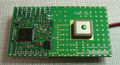
Tiny v2.1 top side view (13mm GPS antenna)
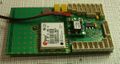
Tiny v2.1 bottom side view


The Tiny v2.1 autopilot uses a single Philips LPC2148 ARM7 based microcontroller. The ARM7 is a low-power 32-bit RISC processor core and the Philips LPC2148 has 512KB on-chip Flash ROM, 40KB RAM and can be clocked at 60MHz.
Although critical control code such as the R/C interface and servo output are well segregated in Paparazzi software and well protected from interference from flaws in the stability/navigation/comm/payload code, great care must be taken when experimenting with new software as some errors can cause a the processor to halt or stall for extended periods causing total loss of control.
Architecture
Pinout
Pins Name and Type are specified with respect to the Autopilot Board

| Pin # | Name | Type | Description | Suggested Color |
|---|---|---|---|---|
| 1 | GND | PWR | common ground | Black |
| 2 | +5V | PWR | 5V Rail from Tiny | Orange |
| 3 | +3.3V | PWR | 3.3V Rail from Tiny | Red |
| 4 | DTR | |||
| 5 | CTS | |||
| 6 | RTS | |||
| 7 | RXD1 | IN | UART1 Serial Input (3.3V level, 5V Tolerant) | Green |
| 8 | TXD1 | OUT | UART1 Serial Output (3.3V level) | Blue |
| Pin # | Name | Type | Description | Suggested Color |
|---|---|---|---|---|
| 1 | GND | PWR | common ground | Black |
| 2 | +3.3V | PWR | 3.3V Rail from Tiny | Red |
| 3 | SSEL | IN | SSP Slave Select. Selects the SSP interface as a slave (SSEL1) | Braun |
| 4 | MOSI | I/O | SPI1 Master Out Slave In. Data output from master or data input to slave | Grey |
| 5 | MISO | I/O | SPI1 Master In Slave Out. Data input to master or data output from slave | Green |
| 6 | DRDY | IN | External interrupt 0 input (EINT0) | Purple |
| 7 | SCK | I/O | SPI0 Serial clock. Clock output from master or input to slave | Yellow |
| Pin # | Name | Type | Description | Suggested Color |
|---|---|---|---|---|
| 1 | GND | PWR | common ground | Black |
| 2 | +5v | PWR | 5V Rail from Tiny to R/C receiver supply | Orange |
| 3 | PPM_IN | IN | PPM Stream from R/C Receiver (5V tolerant) | White |
| 4 | SERV_RST | OUT | external PPM decoder reset (Note 1) | |
| 5 | SERV_CLK | OUT | external PPM decoder clock (Note 1) |
Note 1 : Used only if servos are connected to the R/C receiver
| Pin # | Name | Type | Description | Suggested Color |
|---|---|---|---|---|
| 1 | GND | PWR | common ground | Black |
| 2 | +3.3V | PWR | 3.3V Rail from Tiny | Red |
| 3 | USB+ | I/O | USB bidirectional D+ line | Green |
| 4 | USB- | I/O | USB bidirectional D- line | White |
| 5 | VBUS | IN | Indicates the presence of USB bus power (P0.23) (5V level) | Orange |
| 6 | BUTTON | IN | External Button (+3.3v pullup) | |
| 7 | LED3 | OUT | GPIO (LED #3 command) | |
| 8 | ADC_7 | IN | Analog to Digital Converter Input #7 |
| Pin # | Name | Type | Description | Suggested Color |
|---|---|---|---|---|
| 1 | GND | PWR | common ground | Black |
| 2 | +3.3V | PWR | 3.3V Rail from Tiny | Red |
| 3 | IRV | IN | Vertical IR Sensor signal (Analog to Digital Converter Input #0) | Purple |
| Pin # | Name | Type | Description | Suggested Color |
|---|---|---|---|---|
| 1 | GND | PWR | common ground | Black |
| 2 | +3.3V | PWR | 3.3V Rail from Tiny | Red |
| 3 | ADC_2 | IN | Horizontal IR Sensor signal axis 2 (Analog to Digital Converter Input #2) | Grey |
| 4 | ADC_1 | IN | Horizontal IR Sensor signal axis 1 (Analog to Digital Converter Input #1) | Braun |
| Pin # | Name | Type | Description | Suggested Color |
|---|---|---|---|---|
| 1 | GND | PWR | common ground | Black |
| 2 | +5v | PWR | 5V Rail from Tiny | Orange |
| 3 | +3.3V | PWR | 3.3V Rail from Tiny | Red |
| 4 | ADC_4 | IN | Analog to Digital Converter Input #4 | |
| 5 | ADC_3 | IN | Analog to Digital Converter Input #3 |
| Pin # | Name | Type | Description | Suggested Color |
|---|---|---|---|---|
| 1 | GND | PWR | common ground | Black |
| 2 | +5v | PWR | 5V Rail from Tiny | Orange |
| 3 | +3.3V | PWR | 3.3V Rail from Tiny | Red |
| 4 | ADC_6 | IN | Analog to Digital Converter Input #6 (Maximum input level can be selected with R12 & R14 values) | |
| 5 | ADC_5 | IN | Analog to Digital Converter Input #5 (Maximum input level can be selected with R13 & R15 values) |
| Pin # | Name | Type | Description | Suggested Color |
|---|---|---|---|---|
| 1 | GND | PWR | common ground | Black |
| 2 | +5v | PWR | 5V Rail from Tiny | Orange |
| 3 | +3.3V | PWR | 3.3V Rail from Tiny | Red |
| 4 | BOOT | IN | In-Circuit Serial Programming (ISP) enable (P0.14, +3.3v pullup) (Note 2) | |
| 5 | GPS_RESET | IN | leave unconnected, hold this pin low only for bootloader programming (Note 3) | |
| 6 | TXD0 | OUT | UART0 Serial Output (shared with GPS receiver) | Blue |
| 7 | RXD0 | IN | UART0 Serial Input (shared with GPS receiver) | Green |
Note 2 : Holding this pin low for at least 3mS after a RESET (or power up) instructs the controller to enter programming mode.
Note 3 : MAXIMUM VOLTAGE ON THIS PIN : 1.95V !!!
| Pin # | Name | Type | Description | Suggested Color |
|---|---|---|---|---|
| 1 | GND | PWR | common ground | Black |
| 2 | +5V | PWR | 5V Rail from Tiny | Orange |
| 3 | +3.3V | PWR | 3.3V Rail from Tiny | Red |
| 4 | SDA | I/O | I2C bus Serial DAta | |
| 5 | SCL | I/O | I2C bus Serial CLock |
| Pin # | Name | Type | Description | Suggested Color |
|---|---|---|---|---|
| 1 | GND | PWR | common ground | Black |
| 2 | +5V | PWR | 5V Rail from Tiny | Orange |
| 3 | +3.3V | PWR | 3.3V Rail from Tiny | Red |
| 4 | CAM_SW | OUT | video source/payload selection signal | |
| 5 | SRV_1 | OUT | Servo PWM signal #1 | |
| 6 | SRV_5 | OUT | Servo PWM signal #5 | |
| 7 | AUX | PWR | video/payload switchable 5V power suply |
Schematic

PCB
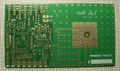
Tiny v2.1 PCB top side view (Olimex)
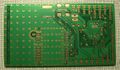
Tiny v2.1 PCB bottom side view (Olimex)

