Tiny v2
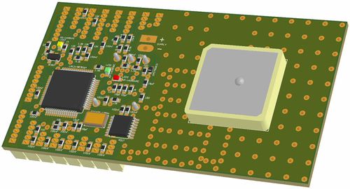
The complete re-design of the popular Tiny autopilot was done on October 9, 2007. The new design is not a bug-fix as no known flaws exist with the current 0.99 and 1.1 versions, so the redesign is performance, easy to use and easy to assemble-oriented !
Hardware Revision History
| Version # | Release Date | Release Notes |
|---|---|---|
| v2.11 | 12/2007 | Bug fix : GPS Reset pin protection (D2) |
| v2.1 | 10/2007 | 3.3V regulator type changed, power switch type changed, connectivity improved |
| v2.0 | 06/2007 | Initial release of Tiny v2 |
Features
- Single LPC2148 MCU
- 8 x Analog input channels 0V - 3.3V (2 channels with optional on-board resistor bridge)
- 1 x 3.3V TTL UART (5V tolerant)
- 8 x PWM outputs
- 1 x R/C receiver PPM frame input
- 1 x SPI bus
- 1 x I2C bus
- 1 x USB (client)
- Integrated GPS receiver and patch antenna (4Hz update)
- 5V/2.5A switching power supply & 3.3V/1A linear regulator
- 3 x status LEDs with attached test point
- ?? grams
- 70.8 x 40mm (smaller then a banking card)
- 2 layers PCB design, 0603 components
The Tiny v2.1 autopilot uses a single Philips LPC2148 ARM7 based microcontroller. The ARM7 is a low-power 32-bit RISC processor core and the Philips LPC2148 has 512KB on-chip Flash ROM, 40KB RAM and can be clocked at 60MHz.
Although critical control code such as the R/C interface and servo output are well segregated in Paparazzi software and well protected from interference from flaws in the stability/navigation/comm/payload code, great care must be taken when experimenting with new software as some errors can cause a the processor to halt or stall for extended periods causing total loss of control.
Feature additions : Tiny 2.1 vs Tiny 1.1
- Hardware flow control on the modem
- The LPC has one "full-featured" serial port and one basic serial port.
- Tiny v1.1 had the full-featured port hard-wired to the GPS in order to leave the basic port open for initial bootloader programming.
- Tiny v2.1 exchange these ports and use the GPS Reset signal to "disconnect" the GPS for the one-time bootloader programming. Hardware flow control on the modem is now possible.
- 5V switching power supply
- The Texas Instruments PTH08080WAH switching 5V/2.25A integrated power supply module greatly simplify manufacturing, reduce costs, and improve performance.
- Tiny v2.1 have a voltage input range of 6.1V → 18V and enough 5V power for large servos, high-power modems and video systems.
- 3.3V linear regulator
- Tiny v2.1 use a LM3940 1A regulator for 5V to 3.3V conversion in a SOT223 standard pinout package which is capable of providing plenty of power to modems or other devices.
- Tests have shown that any device with irregular power consumption can cause significant voltage fluctuations on the critical 3.3V bus.
- Users are advised to use a separate regulator as needed for such devices.
- Video/payload power switch.
- The TPS1100 transistor used on the Tiny v1.1 design has proven extremely useful but is intended for high-speed power switching of motor controllers and occupies a 5mm x 6mm space (SOIC-8).
- The replacement on the new Tiny v2.1 is a current-limiting switch TPS2051B intended for peripheral power control and should protect the 5V supply from voltage sags during the power-up of high capacitance peripherals as well as allow the 5V supply to continue working in the event of a complete short-circuit in the payload.
- TPS2051BDBVR Single 500mA (1A limited) switch in a 3mm x 3mm SOT23-5 package
- GPS ground plane and antenna
- The 13mm antenna on previous Tiny v1.1 proved to be an unworthy exchange of performance for weight. Crude parking-lot tests showed an approximate 3dBi loss (as expected from the data sheets), but the narrow bandwidth of the small antenna made it more sensitive to de-tuning from nearby components in the aircraft. Flight performance was acceptable but poor climb rate calculations were observed with the smaller antenna. Tiny 1.1 users are advised to fit a 20mm antenna.
- Tiny v2.1 use a 18mm x 4mm antenna (20mm x 4mm is possible but no more available) and feature 30% more ground plane area (40 x 40mm).
- GPS Reset
- Occasionally the GPS fails to boot properly, displays very poor S/N ratios, and fails to obtain a valid fix. This may be caused by a slow power-up of the 5V or 3V regulators, or by some unusual EMI that is only present at boot. Usually a simple power cycle will correct the problem but occasionally the receiver seems to use the backup battery to retain the bad state.
- On the Tiny v2.1 design GPS reset is connected to a GPIO pin on the MCU and allow the operator to reset the GPS as needed.
- Headers
- Tiny v2.1 feature revised header layouts on all peripherals.
- The modem header have CTS/RTS/DTR and both 5V and 3.3V supplies.(3.3V is shared with LPC and ADC channels - use with caution and only with very low power modems like the 10mW Xbee).
- The Tiny v1.1 button is removed and it's function is combined on the USB header along with a LED trigger so that indicator, button, and USB can be remotely mounted.
- Vertical Infrared (1 ADC) with 3.3v supply
- Horizontal Infrared (2 ADC) with 3.3v supply
- 2 general purpose ADC with both 3.3v and 5v supplies
- 2 general purpose ADC with optional on-board resistor bridge and both 3.3v and 5v supplies
- Two axis Camera control with two servo signal, vdo switch control, vdo power switch and both 5V and 3.3V supplies
- SPI bus with 3.3V supply
- I2C bus with both 5V and 3V supplies
- Leds & testpoints
- 3 status LEDs with attached test point available on Tiny v2.1 design (instead 2 on Tiny v1.1)
- Components size
- Many users (not only beginners) don't really think that 0402 components on Tiny v1.1 is a great saving from any viewpoint. Even if one saves a little space by using these components, there must still be enough room around to solder it by hand with a soldering iron.
- Tiny v2.1 use 0603 components, the assembly should be a bit more friendly to everyone.
- Layers amount
- Tiny v2.1 2 Layer design (instead 4 Layers on Tiny v1.1) should simplify manufacturing and reduce costs.
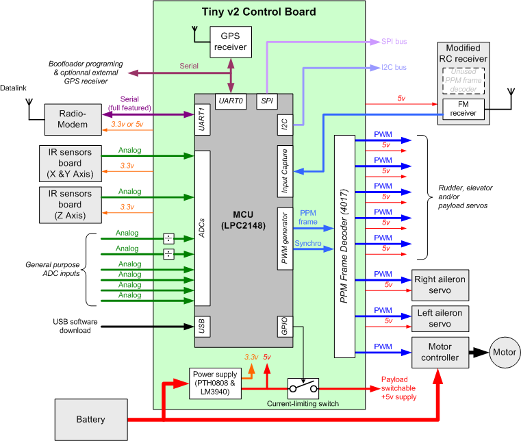
Architecture
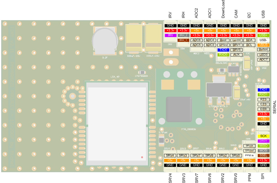
Pinout
Pins Name and Type are specified with respect to the Autopilot Board
| Pin # | Name | Type | Description | Suggested Color |
|---|---|---|---|---|
| 1 | GND | PWR | common ground | Black |
| 2 | +5V | PWR | 5V Rail from Tiny | Orange |
| 3 | +3.3V | PWR | 3.3V Rail from Tiny | Red |
| 4 | DTR | |||
| 5 | CTS | |||
| 6 | RTS | |||
| 7 | RXD1 | IN | UART1 Serial Input (3.3V level, 5V Tolerant) | Green |
| 8 | TXD1 | OUT | UART1 Serial Output (3.3V level) | Blue |
| Pin # | Name | Type | Description | Suggested Color |
|---|---|---|---|---|
| 1 | GND | PWR | common ground | Black |
| 2 | +3.3V | PWR | 3.3V Rail from Tiny | Red |
| 3 | SSEL | IN | SSP Slave Select. Selects the SSP interface as a slave (SSEL1) | Braun |
| 4 | MOSI | I/O | SPI1 Master Out Slave In. Data output from master or data input to slave | Grey |
| 5 | MISO | I/O | SPI1 Master In Slave Out. Data input to master or data output from slave | Green |
| 6 | DRDY | IN | External interrupt 0 input (EINT0) | Purple |
| 7 | SCK | I/O | SPI0 Serial clock. Clock output from master or input to slave | Yellow |
| Pin # | Name | Type | Description | Suggested Color |
|---|---|---|---|---|
| 1 | GND | PWR | common ground | Black |
| 2 | +5v | PWR | 5V Rail from Tiny to R/C receiver supply | Orange |
| 3 | PPM_IN | IN | PPM Stream from R/C Receiver (5V tolerant) | White |
| 4 | SERV_RST | OUT | external PPM decoder reset (Note 1) | |
| 5 | SERV_CLK | OUT | external PPM decoder clock (Note 1) |
Note 1 : Used only if servos are connected to the R/C receiver
| Pin # | Name | Type | Description | Suggested Color |
|---|---|---|---|---|
| 1 | GND | PWR | common ground | Black |
| 2 | +3.3V | PWR | 3.3V Rail from Tiny | Red |
| 3 | USB+ | I/O | USB bidirectional D+ line | Green |
| 4 | USB- | I/O | USB bidirectional D- line | White |
| 5 | VBUS | IN | Indicates the presence of USB bus power (P0.23) (5V level) | Orange |
| 6 | BUTTON | IN | External Button (+3.3v pullup) | |
| 7 | LED3 | OUT | GPIO (LED #3 command) | |
| 8 | ADC_7 | IN | Analog to Digital Converter Input #7 |
| Pin # | Name | Type | Description | Suggested Color |
|---|---|---|---|---|
| 1 | GND | PWR | common ground | Black |
| 2 | +3.3V | PWR | 3.3V Rail from Tiny | Red |
| 3 | IRV | IN | Vertical IR Sensor signal (Analog to Digital Converter Input #0) | Purple |
| Pin # | Name | Type | Description | Suggested Color |
|---|---|---|---|---|
| 1 | GND | PWR | common ground | Black |
| 2 | +3.3V | PWR | 3.3V Rail from Tiny | Red |
| 3 | IRH_2 | IN | Horizontal IR Sensor signal axis 2 (Analog to Digital Converter Input #2) | Grey |
| 4 | IRH_1 | IN | Horizontal IR Sensor signal axis 1 (Analog to Digital Converter Input #1) | Braun |
| Pin # | Name | Type | Description | Suggested Color |
|---|---|---|---|---|
| 1 | GND | PWR | common ground | Black |
| 2 | +5v | PWR | 5V Rail from Tiny | Orange |
| 3 | +3.3V | PWR | 3.3V Rail from Tiny | Red |
| 4 | ADC_4 | IN | Analog to Digital Converter Input #4 | |
| 5 | ADC_3 | IN | Analog to Digital Converter Input #3 |
| Pin # | Name | Type | Description | Suggested Color |
|---|---|---|---|---|
| 1 | GND | PWR | common ground | Black |
| 2 | +5v | PWR | 5V Rail from Tiny | Orange |
| 3 | +3.3V | PWR | 3.3V Rail from Tiny | Red |
| 4 | ADC_6 | IN | Analog to Digital Converter Input #6 (Maximum input level can be selected with R12 value) | |
| 5 | ADC_5 | IN | Analog to Digital Converter Input #5 (Maximum input level can be selected with R13 value) |
| Pin # | Name | Type | Description | Suggested Color |
|---|---|---|---|---|
| 1 | GND | PWR | common ground | Black |
| 2 | +5v | PWR | 5V Rail from Tiny | Orange |
| 3 | +3.3V | PWR | 3.3V Rail from Tiny | Red |
| 4 | BOOT | IN | In-Circuit Serial Programming (ISP) enable (P0.14, +3.3v pullup) (Note 2) | |
| 5 | GPS_RESET | IN | leave unconnected, hold this pin low only for bootloader programming | |
| 6 | TXD0 | OUT | UART0 Serial Output (shared with GPS receiver) | Blue |
| 7 | RXD0 | IN | UART0 Serial Input (shared with GPS receiver) | Green |
Note 2 : Holding this pin low for at least 3mS after a RESET (or power up) instructs the controller to enter programming mode.
| Pin # | Name | Type | Description | Suggested Color |
|---|---|---|---|---|
| 1 | GND | PWR | common ground | Black |
| 2 | +5V | PWR | 5V Rail from Tiny | Orange |
| 3 | +3.3V | PWR | 3.3V Rail from Tiny | Red |
| 4 | SDA | I/O | I2C bus Serial DAta | |
| 5 | SCL | I/O | I2C bus Serial CLock |
| Pin # | Name | Type | Description | Suggested Color |
|---|---|---|---|---|
| 1 | GND | PWR | common ground | Black |
| 2 | +5V | PWR | 5V Rail from Tiny | Orange |
| 3 | +3.3V | PWR | 3.3V Rail from Tiny | Red |
| 4 | CAM_SW | OUT | video source/payload selection signal | |
| 5 | SRV_1 | OUT | Servo PWM signal #1 | |
| 6 | SRV_5 | OUT | Servo PWM signal #5 | |
| 7 | AUX | PWR | video/payload switchable 5V power suply |
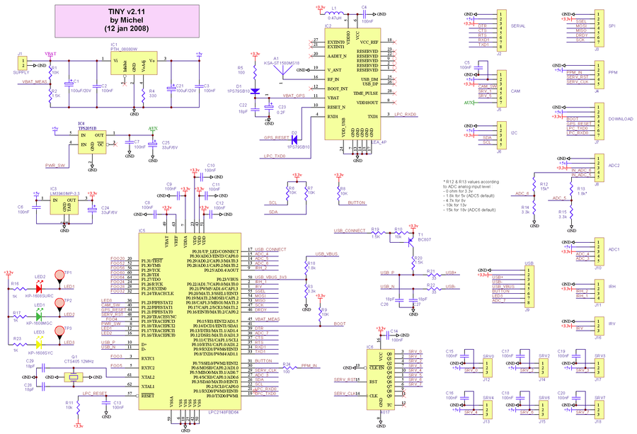
Schematic
PCB
Gerber & Drill Files
Download Tiny v2.11 gerber & drill files (zip)
RS274X, units = Inches, format = 2:5
- Tiny_v2-11.GTO (Top Component Print Layer)
- Tiny_v2-11.GTS (Top Solder Mask)
- Tiny_v2-11.GTL (Top Copper Layer)
- Tiny_v2-11.GBL (Bottom Copper Layer)
- Tiny_v2-11.GBS (Bottom Solder Mask)
- Tiny_v2-11.DRI (NC XY coordinates & Drill tools sizes)
Possible PCB Manufacturers
Mass Production of Tiny V2.11 PCB
To be cost effective, 3 metres square of PCB will be produce & tested! ~ 1000pcs can be made
Each Bare PCB is USD $4 each
Over 10's USD $3
Over 50's USD $2
Next day is ready for shipping!
pls send ur interested to jeff@halfbase.com
Assembly
Components Layout
Bill Of Material
Download Tiny v2.11 Bill Of Material (zipped .xls file)
| Qty | Manufacturer part # | Schematic part name / value | Designator | Description | Manufacturer | Package | Optional | Digikey.com | Other distributor |
|---|---|---|---|---|---|---|---|---|---|
| Resistors | |||||||||
| 2 | ERJ-3EKF33R0V | 33 | R21, R22 | 1/16W, 5% | Panasonic | 0603 | P33HCT-ND | ||
| 2 | ERJ-3EKF1000V | 100 | R5, R24 | 1/16W, 5% | Panasonic | 0603 | P100HCT-ND | ||
| 1 | ERJ-3EKF3300V | 330 | R4 | 1/16W, 5% | Panasonic | 0603 | P330HCT-ND | ||
| 3 | ERJ-3EKF1001V | 1K | R16, R17, R23 | 1/16W, 5% | Panasonic | 0603 | P1.00KHCT-ND | ||
| 3 | ERJ-3EKF1501V | 1.5K | R2, R19, R20 | 1/16W, 5% | Panasoni | 0603 | P1.50KHCT-ND | ||
| 2 | ERJ-3EKF1801V | 1.8k (see note1) | R13,R18 | 1/16W, 5% | Panasonic | 0603 | P1.8KHCT-ND | ||
| 3 | ERJ-3EKF3301V | 3.3K | R3, R14, R15 | 1/16W, 5% | Panasonic | 0603 | P3.3KHCT-ND | ||
| 7 | ERJ-3EKF1002V | 10K | R1, R6 to R11 | 1/16W, 5% | Panasonic | 0603 | P10.0KHCT-ND | ||
| 1 | ERJ-3EKF1502V | 15K (see note2) | R12 | 1/16W, 5% | Panasonic | 0603 | P15.0KHCT-ND | ||
| Capacitors | |||||||||
| 5 | C0603C180J5GAC | 18pF | C22, C26 to C29 | 50V, 5% | Kemet | 0603 | 399-1052-1-ND | ||
| 19 | C0603C104K5RAC | 100nF | C2 to C20 | 50V, 10% | Kemet | 0603 | 399-5089-1-ND | ||
| 2 | T520A336M006ATE070 | 33uF/6V | C24, C25 | SMD tantalum capacitor | Kemet | A case (EIA 3216-18) | 399-4719-1-ND | ||
| 2 | TAJD107K020R | 100uF/20V | C1, C21 | SMD tantalum capacitor | AVX Corp. | D case (EIA 7343-31) | 478-1724-1-ND | ||
| 1 | EEC-EN0F204JK | 0.2F | C23 | SMD double layer capacitor (Goldcap) | Panasonic | specific | P11070CT-ND | ||
| Inductors | |||||||||
| 1 | MLF2012DR47K | 0.47uH | L1 | SMD Inductor | TDK | 0805 | 445-1043-1-ND | ||
| Semiconductors | |||||||||
| 2 | 1PS79SB10 | 1PS79SB10 | D1, D2 | Schottky diode 0.2A/30v | NXP | SOD523 (EIA SC79) | 1PS79SB10 T/R-ND | ||
| 1 | LM3940IMP-3.3 | LM3940IMP-3.3 | IC3 | 1A low dropout regulator for 5V to 3.3V conversion | National Semic. | SOT223 | LM3940IMP-3.3CT-ND | ||
| 1 | TPS2051BDBV | TPS2051B | IC4 | Current Limited Power Distribution Switch | Texas Instr. | SOT23-5 | yes | 296-21265-1-ND | |
| 1 | LPC2148FBD64 | LPC2148FBD64 | IC5 | Single-chip ARM7 32-bit microcontroller | NXP | LQFP64 | 568-1765-ND | ||
| 1 | CD4017BPW | 4017 | IC6 | Decade Counter/Divider with 10 Decoded Outputs | Texas Instr. | TSSOP16 | 296-14252-1-ND | ||
| 1 | APT1608MGC | KP-1608MGC | LED1 | SMD Chip Green LED Lamp | Kingbright | 0603 | 754-1118-1-ND | ||
| 1 | APT1608SURCK | KP-1608SURC | LED2 | SMD Chip Red LED Lamp | Kingbright | 0603 | yes | 754-1123-1-ND | |
| 1 | APT1608SYCK | KP-1608SYC | LED3 | SMD Chip Yellow LED Lamp | Kingbright | 0603 | yes | 754-1124-1-ND | |
| 1 | BC807-40 | BC807 | T1 | PNP general purpose transistor | NXP | SOT23 | 568-1629-1-ND | ||
| Modules | |||||||||
| 1 | PTH08080WAH | PTH_08080W | IC1 | 2.25A Wide-input adjustable switching regulator | Texas Instr. | specific | 296-20432-ND | ||
| 1 | LEA-4P-0-000-0 | LEA_4P | IC2 | ublox | specific | N/A | (u-blox.com, see note 3) | ||
| Connectors | |||||||||
| 7 | 53047-0310 | SRV0, SRV4, SRV2, SRV6, IRV, SRV3, SRV7 | J12 to J18 | Picoblade 3 pins 1.25mm straight header | Molex | specific | WM1732-ND | ||
| 1 | 53047-0410 | IRH | J11 | Picoblade 4 pins 1.25mm straight header | Molex | specific | WM1733-ND | ||
| 4 | 53047-0510 | PPM,I2C,ADC2,ADC1 | J4, J6, J8, J10 | Picoblade 5 pins 1.25mm straight header | Molex | specific | J6,J8,J10 | WM1734-ND | |
| 3 | 53047-0710 | SPI,CAM,DOWNLOAD | J3, J5, J7 | Picoblade 7 pins 1.25mm straight header | Molex | specific | J3,J5 | WM1736-ND | |
| 2 | 53047-0810 | SERIAL,USB | J2, J9 | Picoblade 8 pins 1.25mm straight header | Molex | specific | WM1737-ND | ||
| Other | |||||||||
| 1 | 405C35B12M00000 | CTS405 12MHz | Q1 | SMD 12MHz Quartz Crystal | CTS | specific | CTX639CT-ND | ||
| 1 | KSA-ST1580MS18 | KSA-ST1580MS18 | A1 | 18x18mm ceramic Patch Antenna | Sangshin | specific | - | N/A | KSA-ST1580MS18 (rfmw.com) |
| ANA1580T18D4 | Emtac | ANA1580T18D4 (transplantgps.com) | |||||||
Note 1 :
R13 calculated according attached ADC5 desired input level :
- 3.3v ⇒ 0
- 5v ⇒ 1.8k (default)
- 8v ⇒ 4.7k
- 13v ⇒ 10k
- 18v ⇒ 15K
- Other ⇒ R13 = (Vin - 3.3) x 1000
Note 2 : R12 calculated according attached ADC6 desired input level :
- 3.3v ⇒ 0
- 5v ⇒ 1.8k
- 8v ⇒ 4.7k
- 13v ⇒ 10k
- 18v ⇒ 15K (default)
- Other ⇒ R13 = (Vin - 3.3) x 1000
Note 3 : For sales make contact with Ublox distributor in the appropriate region (http://www.u-blox.com/disti/index.html)
Downloads
Source files
Gerber & Drill files
Assembly files


